SBOS704B May 2015 – March 2016 DRV421
PRODUCTION DATA.
- 1 Features
- 2 Applications
- 3 Description
- 4 Revision History
- 5 Pin Configuration and Functions
- 6 Specifications
-
7 Detailed Description
- 7.1 Overview
- 7.2 Functional Block Diagram
- 7.3
Feature Description
- 7.3.1 Fluxgate Sensor
- 7.3.2 Integrator-Filter Function and Compensation Loop Stability
- 7.3.3 H-Bridge Driver for Compensation Coil
- 7.3.4 Shunt Sense Amplifier
- 7.3.5 Overrange Comparator
- 7.3.6 Voltage Reference
- 7.3.7 Overload Detection and Control
- 7.3.8 Magnetic Core Demagnetization
- 7.3.9 Search Function
- 7.3.10 Error Flag
- 7.4 Device Functional Modes
- 8 Application and Implementation
- 9 Power-Supply Recommendations
- 10Layout
- 11Device and Documentation Support
- 12Mechanical, Packaging, and Orderable Information
Package Options
Mechanical Data (Package|Pins)
- RTJ|20
Thermal pad, mechanical data (Package|Pins)
- RTJ|20
Orderable Information
8 Application and Implementation
NOTE
Information in the following applications sections is not part of the TI component specification, and TI does not warrant its accuracy or completeness. TI’s customers are responsible for determining suitability of components for their purposes. Customers should validate and test their design implementation to confirm system functionality.
8.1 Application Information
8.1.1 Magnetic Core Design
The high sensitivity, low offset, and low noise of the DRV421 fluxgate sensor enable a high-performance closed-loop current sensor module. For good module performance, an appropriate magnetic core design is required.
Table 3 lists the DRV421 and magnetic core specifications with relation to the overall current module specifications.
Table 3. Current-Sensor Module Performance versus
DRV421 Specifications and Magnetic Core Performance
| CURRENT SENSOR MODULE PARAMETER | PERFORMANCE DETERMINED BY: |
|---|---|
| Offset and offset drift | DRV421 fluxgate sensor front-end: offset and offset drift |
| Offset on start-up and after overload condition |
Magnetic core: magnetization (see the Magnetic Core Demagnetization section) |
| Noise | DRV421 fluxgate sensor front-end: noise |
| Linearity error | DRV421 fluxgate sensor front-end: AC open-loop gain |
| Gain error | Magnetic core: Permeability, geometry, and actual number of compensation coil windings |
| Measurement range | 1) DRV421 fluxgate sensor front-end: H-bridge peak current 2) Compensation coil: number of windings and resistance 3) Value of the external shunt resistor |
| Neighbor-current rejection (crosstalk) |
Magnetic core: permeability, sensor gap design, and magnetic shielding |
| Bandwidth and gain flatness | 1) DRV421 fluxgate sensor front-end: AC open-loop gain setting 2) Magnetic core: high-frequency behavior of the core and inductance of the compensation coil 3) Value of the external shunt resistor |
| Common-mode current rejection (for fault current sensors) |
Magnetic core: permeability, actual position of the primary current conductors, and magnetic shielding |
For further details, see application report SLOA223, Designing with the DRV421: Closed Loop Current Sensor Specifications.
8.1.2 Protection Recommendations
Inputs AINP and AINN require external protection to limit the voltage swing to within 6 V beyond both supply rails. Driver outputs ICOMP1 and ICOMP2 handle high-current pulses protected by internal clamp circuits to the supply voltage. If large magnitude overcurrents are expected, connect external Schottky diodes to the supply rails to protect the DRV421 from damage.
CAUTION
Large overcurrents may drive the power supply above the normal operating voltage. Route large overcurrent pulses away from the device using diodes connected to the supply, as shown in the typical application on the front page. To prevent these pulses from driving up the supply voltage, and prevent damage to the DRV421 and other components in the circuit, use an additional supply clamp, as shown in Figure 64. All other pins offer standard protection; see the Absolute Maximum Ratings.
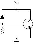 Figure 64. Additonal Supply Clamp for the DRV421
8.2 Typical Application
8.2.1 Closed-Loop Current Sensing Module
Closed-loop current sensor modules (Figure 65) measure currents over a wide frequency range, including dc currents. These sensor modules offer a contact-free sensing method and excellent galvanic isolation performance, combined with high resolution, accuracy, and reliability. The DRV421 is designed for use in this kind of application.
At dc and in low-frequency range, the magnetic field induced by the primary current is sensed by the DRV421 fluxgate sensor. The sensed signal is filtered by the DRV421 and the internal H-bridge driver generates a proportional compensation current. The compensation current flows through the compensation coil, and generates a magnetic field. This magnetic field drives the original magnetic flux in the core back to zero. The value of this magnetic field is increased by the number of compensation coil windings. Therefore, use Equation 1 to calculate the required compensation current for a given primary current.
At higher frequencies, the magnetic field induced by the primary current directly couples into the compensation coil and generates a current. The low impedance of the H-bridge driver does not influence the value of this current. Also in this case, the value of the compensation current is the value of the primary current divided by the number of compensation coil windings.
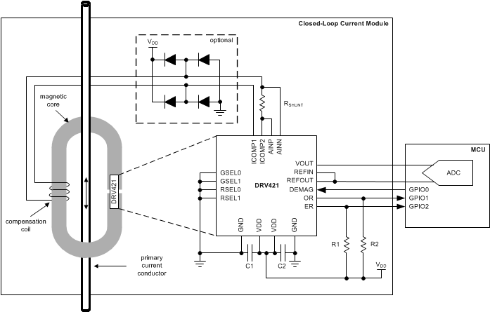 Figure 65. Closed-Loop Current Sensing Module
8.2.1.1 Design Requirements
A closed-loop current sensing module contains the DRV421, the magnetic core with a compensation coil, and a shunt resistor. To increase the robustness of the module to high primary current peaks, use additional protection diodes. See application report SLOA223, Designing with the DRV421: Closed Loop Current Sensor Specifications, for additional information on the magnetic core and compensation coil design. The DRV421 output voltage is calculated as described in Equation 6:

where
- IPRIM = primary current value
- NPRIM = the number of windings of the primary current conductor
- NWINDING = the number of windings of the compensation coil
- RSHUNT = shunt resistor value
- G = shunt sense amplifier gain; default value is 4
8.2.1.2 Detailed Design Procedure
The compensation current creates a voltage drop across the shunt resistor. The maximum shunt resistor value is limited by supply voltage VDD, the compensation current range, and the resistance of the compensation coil, as described in Equation 7:

The voltage drop across the shunt resistor is sensed by the DRV421 shunt sense amplifier with a gain of four. For proper operation, keep the resulting output voltage at VOUT pin within the voltage output swing range specified in the Electrical Characteristics.
8.2.1.3 Application Curves
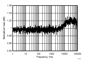
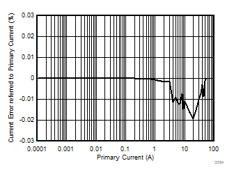
8.2.2 Differential Closed-Loop Current Sensing Module
The differential closed-loop current sensing module (Figure 68) measures the difference between two or more currents. Typical end-applications for such modules are leakage or residual current sensors. The high sensitivity of the fluxgate sensor and the low temperature drift make the DRV421 a suitable choice for this type of modules. The principle operation is the same as that of the closed-loop current module described in the Closed-Loop Current Sensing Module section. The compensation current corresponds to the current difference between the primary conductors.
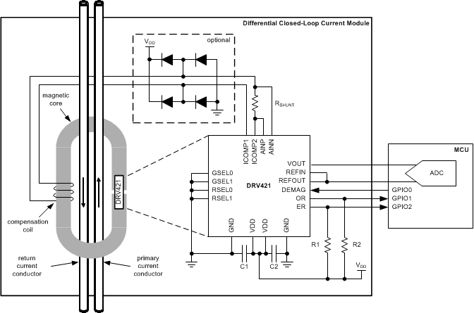 Figure 68. Differential Closed-Loop Current Sensing Module
8.2.2.1 Design Requirements
As with the previous application, the compensation current creates a voltage drop across the shunt resistor. The maximum shunt resistor value is limited by supply voltage VDD, the compensation current range, and the resistance of the compensation coil; see Equation 7.
However, in applications that sense leakage or residual currents, the difference between the primary currents is zero in normal operation. In fault condition only, there is a small difference current that is sensed in order to shut down the system to prevent damage to the device or the user. In this case, the compensation current is also very low, usually only in the range of few mA. Therefore, use a higher shunt resistor value in this case to support high sensitivity on system level. Consider the impact of shunt resistor value on gain and gain flatness as decribed in application report SLOA223, Designing with the DRV421: Closed Loop Current Sensor Specifications.
8.2.2.2 Detailed Design Procedure
For differential current sensing modules with a large shunt resistor and medium compensation coil inductance, use the gain setting that features the higher cross-over frequency of 3.8 kHz: GSEL[1:0] = 01.
8.2.2.3 Application Curve
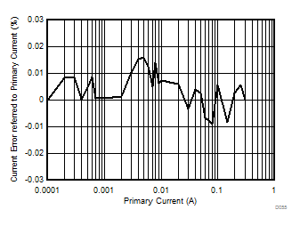
Differential Closed-Loop Current Sensing Module
8.2.3 Using the DRV421 in ±15-V Sensor Applications
The DRV421 is designed for 3.3-V or 5-V nominal operation. To support a wider module current range, the device is also used in ±15-V application, as shown in Figure 70. In this application, an external regulator generates the 5-V supply for the DRV421. An additional external ±15-V power driver stage drives the compensation coil. These techniques allow the design of exceptionally precise and stable ±15-V current-sense modules.
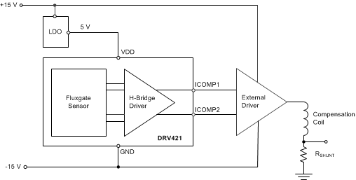 Figure 70. ±15-V Current-Sense Modules