SBOS988A August   2019  – April 2020 DRV425-Q1

PRODUCTION DATA.  

  1. Features
  2. Applications
  3. Description
    1.     Device Images
      1.      Simplified Schematic
  4. Revision History
  5. Pin Configuration and Functions
    1.     Pin Functions
  6. Specifications
    1. 6.1 Absolute Maximum Ratings
    2. 6.2 ESD Ratings
    3. 6.3 Recommended Operating Conditions
    4. 6.4 Thermal Information
    5. 6.5 Electrical Characteristics
    6. 6.6 Typical Characteristics
  7. Detailed Description
    1. 7.1 Overview
    2. 7.2 Functional Block Diagram
    3. 7.3 Feature Description
      1. 7.3.1 Fluxgate Sensor Front-End
        1. 7.3.1.1 Fluxgate Sensor
        2. 7.3.1.2 Bandwidth
        3. 7.3.1.3 Differential Driver for the Internal Compensation Coil
        4. 7.3.1.4 Magnetic Field Range, Overrange Indicator, and Error Flag
      2. 7.3.2 Shunt-Sense Amplifier
      3. 7.3.3 Voltage Reference
      4. 7.3.4 Low-Power Operation
    4. 7.4 Device Functional Modes
  8. Application and Implementation
    1. 8.1 Application Information
    2. 8.2 Typical Applications
      1. 8.2.1 Linear Position Sensing
        1. 8.2.1.1 Design Requirements
        2. 8.2.1.2 Detailed Design Procedure
        3. 8.2.1.3 Application Curves
      2. 8.2.2 Current Sensing in Busbars
        1. 8.2.2.1 Design Requirements
        2. 8.2.2.2 Detailed Design Procedure
        3. 8.2.2.3 Application Curves
  9. Power Supply Recommendations
    1. 9.1 Power Supply Decoupling
    2. 9.2 Power-On Start-Up and Brownout
    3. 9.3 Power Dissipation
      1. 9.3.1 Thermal Pad
  10. 10Layout
    1. 10.1 Layout Guidelines
    2. 10.2 Layout Example
  11. 11Device and Documentation Support
    1. 11.1 Documentation Support
      1. 11.1.1 Related Documentation
    2. 11.2 Receiving Notification of Documentation Updates
    3. 11.3 Support Resources
    4. 11.4 Trademarks
    5. 11.5 Electrostatic Discharge Caution
    6. 11.6 Glossary
  12. 12Mechanical, Packaging, and Orderable Information

Package Options

Mechanical Data (Package|Pins)
Thermal pad, mechanical data (Package|Pins)
Orderable Information

Low-Power Operation

In applications with low-bandwidth or low sample-rate requirements, significantly reduce the average power dissipation of the DRV425-Q1 by powering down the device between measurements. The DRV425-Q1 requires 300 μs to fully settle the analog output VOUT, as shown in Figure 66. To minimize power dissipation, power down the device immediately after the ADC acquires the sample.
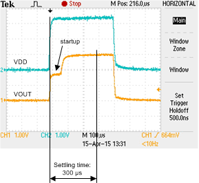
DRV425-Q1 ai_low-power_bos729.gifFigure 66. Settling Time of the DRV425-Q1 VOUT Output