SLIS162I December   2014  – February 2023 DRV5013-Q1

PRODUCTION DATA  

  1. Features
  2. Applications
  3. Description
  4. Revision History
  5. Pin Configuration and Functions
  6. Specifications
    1. 6.1 Absolute Maximum Ratings
    2. 6.2 ESD Ratings
    3. 6.3 Recommended Operating Conditions
    4. 6.4 Thermal Information
    5. 6.5 Electrical Characteristics
    6. 6.6 Switching Characteristics
    7. 6.7 Magnetic Characteristics
    8. 6.8 Typical Characteristics
  7. Detailed Description
    1. 7.1 Overview
    2. 7.2 Functional Block Diagram
    3. 7.3 Feature Description
      1. 7.3.1 Field Direction Definition
      2. 7.3.2 Device Output
      3. 7.3.3 Power-On Time
      4. 7.3.4 Output Stage
      5. 7.3.5 Protection Circuits
        1. 7.3.5.1 Overcurrent Protection (OCP)
        2. 7.3.5.2 Load Dump Protection
        3. 7.3.5.3 Reverse Supply Protection
    4. 7.4 Device Functional Modes
  8. Application and Implementation
    1. 8.1 Application Information
    2. 8.2 Typical Applications
      1. 8.2.1 Standard Circuit
        1. 8.2.1.1 Design Requirements
        2. 8.2.1.2 Detailed Design Procedure
          1. 8.2.1.2.1 Configuration Example
        3. 8.2.1.3 Application Curves
      2. 8.2.2 Alternative Two-Wire Application
        1. 8.2.2.1 Design Requirements
        2. 8.2.2.2 Detailed Design Procedure
    3. 8.3 Power Supply Recommendations
    4. 8.4 Layout
      1. 8.4.1 Layout Guidelines
      2. 8.4.2 Layout Example
  9. Device and Documentation Support
    1. 9.1 Device Support
      1. 9.1.1 Device Nomenclature
      2. 9.1.2 Device Markings
    2. 9.2 Receiving Notification of Documentation Updates
    3. 9.3 Support Resources
    4. 9.4 Trademarks
    5. 9.5 Electrostatic Discharge Caution
    6. 9.6 Glossary
  10. 10Mechanical, Packaging, and Orderable Information

Package Options

Mechanical Data (Package|Pins)
Thermal pad, mechanical data (Package|Pins)
Orderable Information

Output Stage

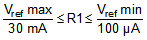
#SLIS1507131 shows the DRV5013-Q1 open-drain NMOS output structure, rated to sink up to 30 mA of current. For proper operation, use #SLIS1505991 to calculate the value of pullup resistor R1.

Equation 1. GUID-3FB5AF64-D19A-474D-B307-4ECB0CF03C01-low.gif

The size of R1 is a tradeoff between the OUT rise time and the current when OUT is pulled low. A lower current is generally better, however faster transitions and bandwidth require a smaller resistor for faster switching.

In addition, make sure that the value of R1 > 500 Ω so that the output driver can pull the OUT pin close to GND.

Note:

Vref is not restricted to VCC. The allowable voltage range of this pin is specified in the GUID-720FE3D7-33A2-49DE-AAD7-DE9137C81B16.html#TITLE-SLIS150SLIS1504651.

GUID-5AA9A189-1EE2-4689-B53B-F572693502C3-low.gifFigure 7-7 NMOS Open-Drain Output

Select a value for C2 based on the system bandwidth specifications as shown in #SLIS1501741.

Equation 2. GUID-979C48D1-3A70-4B13-A944-9444D02F125D-low.gif

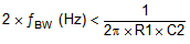
Most applications do not require this C2 filtering capacitor.