SLOS690C December   2010  – July 2016 DRV612

UNLESS OTHERWISE NOTED, this document contains PRODUCTION DATA.  

  1. Features
  2. Applications
  3. Description
  4. Revision History
  5. Device Comparison Table
  6. Pin Configuration and Functions
  7. Specifications
    1. 7.1 Absolute Maximum Ratings
    2. 7.2 ESD Ratings
    3. 7.3 Recommended Operating Conditions
    4. 7.4 Thermal Information
    5. 7.5 Electrical Characteristics
    6. 7.6 Electrical Characteristics, Line Driver
    7. 7.7 Programmable Gain Settings
    8. 7.8 Typical Characteristics
  8. Parameter Measurement Information
  9. Detailed Description
    1. 9.1 Overview
    2. 9.2 Functional Block Diagram
    3. 9.3 Feature Description
      1. 9.3.1 Line Driver Amplifiers
    4. 9.4 Device Functional Modes
      1. 9.4.1 Internal Undervoltage Detection
      2. 9.4.2 Pop-Free Power Up
  10. 10Application and Implementation
    1. 10.1 Application Information
      1. 10.1.1 Capacitive Load
    2. 10.2 Typical Application
      1. 10.2.1 Design Requirements
      2. 10.2.2 Detailed Design Procedure
        1. 10.2.2.1 Component Selection
          1. 10.2.2.1.1 Charge Pump Flying Capacitor and VSS Capacitor
          2. 10.2.2.1.2 Decoupling Capacitors
          3. 10.2.2.1.3 Gain-Setting
          4. 10.2.2.1.4 Input-Blocking Capacitors
      3. 10.2.3 Application Curves
  11. 11Power Supply Recommendations
  12. 12Layout
    1. 12.1 Layout Guidelines
      1. 12.1.1 Footprint Compatible With TPA6139A2
    2. 12.2 Layout Examples
  13. 13Device and Documentation Support
    1. 13.1 Device Support
      1. 13.1.1 Development Support
    2. 13.2 Documentation Support
      1. 13.2.1 Related Documentation
    3. 13.3 Receiving Notification of Documentation Updates
    4. 13.4 Community Resources
    5. 13.5 Trademarks
    6. 13.6 Electrostatic Discharge Caution
    7. 13.7 Glossary
  14. 14Mechanical, Packaging, and Orderable Information

Package Options

Mechanical Data (Package|Pins)
Thermal pad, mechanical data (Package|Pins)
Orderable Information

12 Layout

12.1 Layout Guidelines

A proposed layout for the DRV612 can be seen in the DRV612EVM User's Guide, and the Gerber files can be downloaded from focus.ti.com. To access this information, open the DRV612 product folder and look in the Tools and Software folder.

Ground traces are recommended to be routed as a star ground to minimize hum interference. The VDD and VSS decoupling capacitors and the charge-pump capacitors must be connected with short traces.

12.1.1 Footprint Compatible With TPA6139A2

The DRV612 stereo line driver is pin compatible with the headphone amplifier TPA6139A2. Therefore, a single PCB layout can be used with stuffing options for different board configurations.

DRV612 foot_print_los690.gif Figure 12. DRV612 and TPA6139A2 Pin Compatibility

12.2 Layout Examples

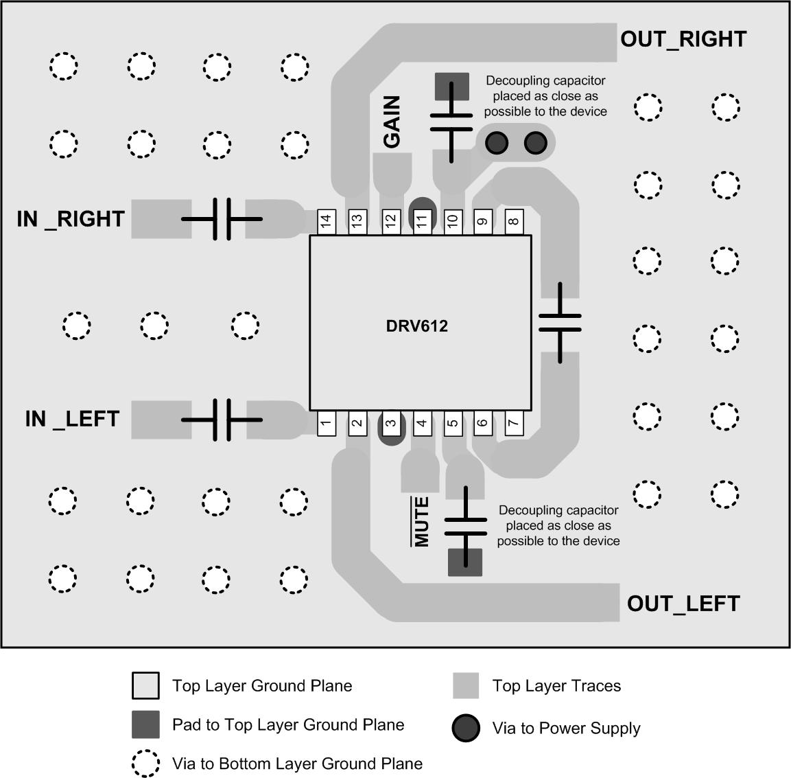
DRV612 DRV612_LayoutExample_TSSOP.gif Figure 13. TSSOP Package Layout
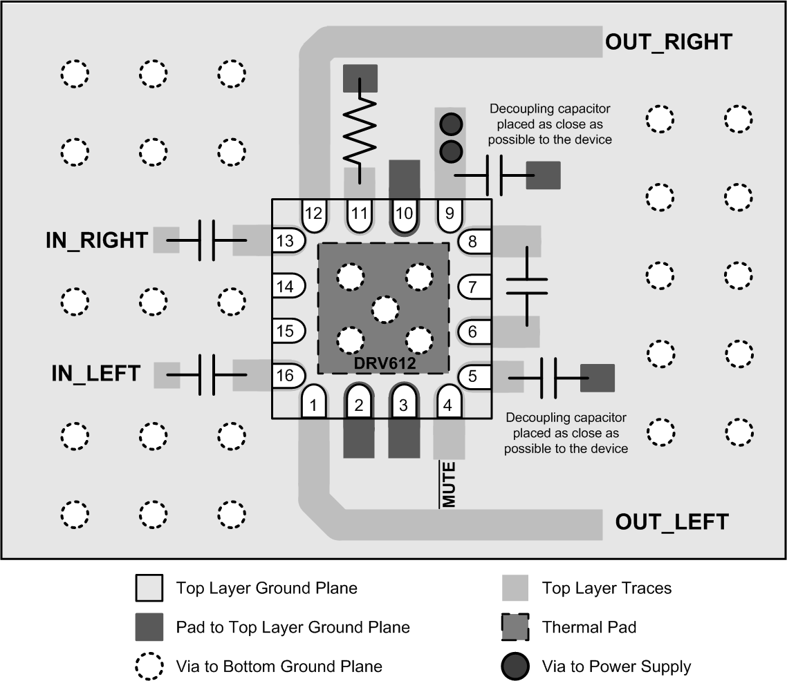
DRV612 DRV612_LayoutExample_QFN.gif Figure 14. VQFN Package Layout