SLOS690C December 2010 – July 2016 DRV612
UNLESS OTHERWISE NOTED, this document contains PRODUCTION DATA.
- 1 Features
- 2 Applications
- 3 Description
- 4 Revision History
- 5 Device Comparison Table
- 6 Pin Configuration and Functions
- 7 Specifications
- 8 Parameter Measurement Information
- 9 Detailed Description
- 10Application and Implementation
- 11Power Supply Recommendations
- 12Layout
- 13Device and Documentation Support
- 14Mechanical, Packaging, and Orderable Information
Package Options
Mechanical Data (Package|Pins)
Thermal pad, mechanical data (Package|Pins)
- RGT|16
Orderable Information
7 Specifications
7.1 Absolute Maximum Ratings
over operating free-air temperature range (unless otherwise noted)(1)| MIN | MAX | UNIT | |||
|---|---|---|---|---|---|
| Voltage | Input, VI | VSS – 0.3 | VDD + 0.3 | V | |
| VDD to GND | –0.3 | 4 | |||
| MUTE to GND | –0.3 | VDD + 0.3 | |||
| Temperature | Maximum operating junction temperature, TJ | –40 | 150 | °C | |
| Storage temperature, Tstg | –65 | 150 | |||
(1) Stresses beyond those listed under Absolute Maximum Ratings may cause permanent damage to the device. These are stress ratings only, and functional operation of the device at these or any other conditions beyond those indicated under Recommended Operating Conditions is not implied. Exposure to absolute-maximum-rated conditions for extended periods may affect device reliability.
7.2 ESD Ratings
| VALUE | UNIT | ||||
|---|---|---|---|---|---|
| DRV612 in the PW Package | |||||
| V(ESD) | Electrostatic discharge | Human-body model (HBM), per ANSI/ESDA/JEDEC JS-001(1) | All pins except Pins 2 and 13 | ±4000 | V |
| Pins 2 and 13 | ±8000 | ||||
| Charged-device model (CDM), per JEDEC specification JESD22-C101(2) | ±1500 | ||||
| DRV612 in the RGT Package | |||||
| V(ESD) | Electrostatic discharge | Human-body model (HBM), per ANSI/ESDA/JEDEC JS-001(1) | All pins except Pins 1 and 12 | ±4000 | V |
| Pins 1 and 12 | ±8000 | ||||
| Charged-device model (CDM), per JEDEC specification JESD22-C101(2) | ±1500 | ||||
(1) JEDEC document JEP155 states that 500-V HBM allows safe manufacturing with a standard ESD control process.
(2) JEDEC document JEP157 states that 250-V CDM allows safe manufacturing with a standard ESD control process.
7.3 Recommended Operating Conditions
over operating free-air temperature range unless otherwise noted| MIN | NOM | MAX | UNIT | |||
|---|---|---|---|---|---|---|
| VDD | Supply voltage, DC | 3 | 3.3 | 3.6 | V | |
| RL | Load resistance | 600 | 10000 | Ω | ||
| VIL | Low-level input voltage, MUTE | 38% | 40% | 43% | VDD | |
| VIH | High-level input voltage, MUTE | 57% | 60% | 66% | VDD | |
| TA | Free-air temperature | 0 | 25 | 85 | °C | |
7.4 Thermal Information
| THERMAL METRIC(1) | DRV612 | UNIT | ||
|---|---|---|---|---|
| PW (TSSOP) | RGT (VQFN) | |||
| 14 PINS | 16 PINS | |||
| RθJA | Junction-to-ambient thermal resistance | 130 | 52 | °C/W |
| RθJC(top) | Junction-to-case (top) thermal resistance | 49 | 71 | °C/W |
| RθJB | Junction-to-board thermal resistance | 63 | 26 | °C/W |
| ψJT | Junction-to-top characterization parameter | 3.6 | 3 | °C/W |
| ψJB | Junction-to-board characterization parameter | 62 | 26 | °C/W |
| RθJC(bot) | Junction-to-case (bottom) thermal resistance | — | — | °C/W |
(1) For more information about traditional and new thermal metrics, see the Semiconductor and IC Package Thermal Metrics application report.
7.5 Electrical Characteristics
VDD = 3.3 V, RLD = 5 kΩ, TA = 25°C, and charge pump (CCP) = 1 μF (unless otherwise noted)| PARAMETER | TEST CONDITIONS | MIN | TYP | MAX | UNIT | |
|---|---|---|---|---|---|---|
| |VOS| | Output offset voltage | VDD = 3.3 V, input ac-coupled | 0.5 | 1 | mV | |
| PSRR | Power-supply rejection ratio | 70 | 80 | dB | ||
| VOH | High-level output voltage | VDD = 3.3 V | 3.1 | V | ||
| VOL | Low-level output voltage | VDD = 3.3 V | –3.05 | V | ||
| Vuvp_on | VDD, undervoltage detection | 2.8 | V | |||
| Vuvp_hysteresis | VDD, undervoltage detection, hysteresis | 200 | mV | |||
| FCP | Charge-pump switching frequency | 350 | kHz | |||
| |IIH| | High-level input current, MUTE | VDD = 3.3 V, VIH = VDD | 1 | µA | ||
| |IIL| | Low-level input current, MUTE | VDD = 3.3 V, VIL = 0 V | 1 | µA | ||
| I(VDD) | Supply current, no load | VDD, MUTE = 3.3 V | 18 | mA | ||
| Supply current, MUTED | VDD = 3.3 V, MUTE = GND | 18 | mA | |||
| TSD | Thermal shutdown | 150 | °C | |||
| Thermal shutdown hysteresis | 15 | °C | ||||
7.6 Electrical Characteristics, Line Driver
VDD = 3.3 V, RLOAD = 10 kΩ, TA = 25°C, charge pump (CCP) = 1 µF, and 1× gain select (unless otherwise noted)| PARAMETER | TEST CONDITIONS | MIN | TYP | MAX | UNIT | |
|---|---|---|---|---|---|---|
| VO | Output voltage, outputs in phase | 1% THD+N, f = 1 kHz, 10 -kΩ load | 2.2 | Vrms | ||
| THD+N | Total harmonic distortion plus noise | f = 1 kHz, 10-kΩ load, VO = 2 Vrms | 0.007% | |||
| SNR | Signal-to-noise ratio | A-weighted, AES17 filter, 2 Vrms ref | 105 | dB | ||
| DNR | Dynamic range | A-weighted, AES17 filter, 2 Vrms ref | 105 | dB | ||
| Vn | Noise voltage | A-weighted, AES17 filter | 12 | μV | ||
| Zo | Output impedance when muted | MUTE = GND | 0.07 | 1 | Ω | |
| Input-to-output attenuation when muted | 1 Vrms, 1-kHz input | 80 | dB | |||
| Slew rate | 4.5 | V/μs | ||||
| GBW | Unity-gain bandwidth | 8 | MHz | |||
| Crosstalk, line L-R and R-L | 10-kΩ load, VO = 2 Vrms | –91 | dB | |||
| Ilimit | Current limit | VDD = 3.3 V | 25 | mA | ||
7.7 Programmable Gain Settings
VDD = 3.3 V, Rload = 10 kΩ, TA = 25°C, Charge pump: CCP = 1 μF, 1× gain select (unless otherwise noted)(1)(2)(2) Gain setting is latched during power up.
7.8 Typical Characteristics
VDD = 3.3 V, TA = 25°C, RL = 2.5 kΩ, CPUMP = C(VSS) = 1 µF, and Gain = –2 V/V (unless otherwise noted) Figure 1. THD+N vs Output Voltage 3.3 V, 10 kΩ, 1 kHz
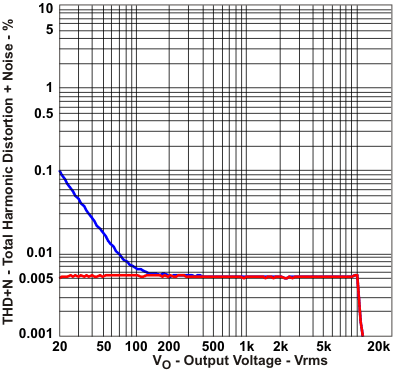
Blue: 10-µF ceramic AC-coupling capacitor.
Red: 10-µF electrolytic AC-coupling capacitor.
Figure 3. THD+N vs Frequency 3.3 V, 10-kΩ Load, 2 Vrms
Red: 10-µF electrolytic AC-coupling capacitor.
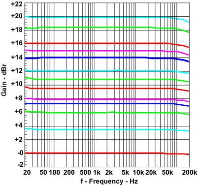 Figure 5. Gain vs Frequency for the Different Gain Settings
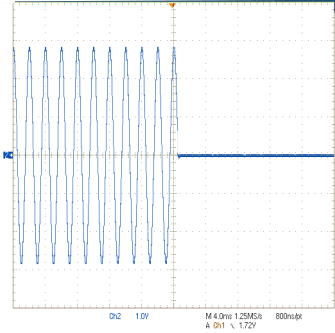 Figure 7. Play to Mute
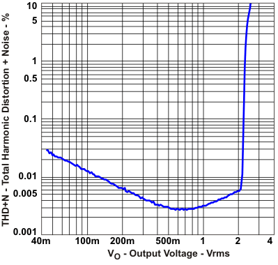 Figure 2. THD+N vs Output Voltage 3.3 V, 600-Ω Load, 1 kHz
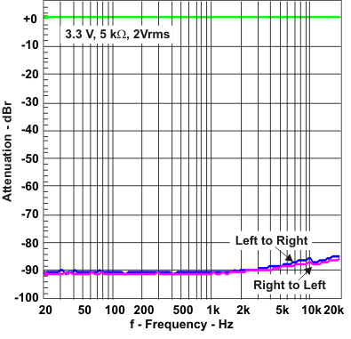
Blue: L to R
Red: R to L
Figure 4. Channel Separation 3.3 V, 5-kΩ Load, 2 Vrms
Red: R to L
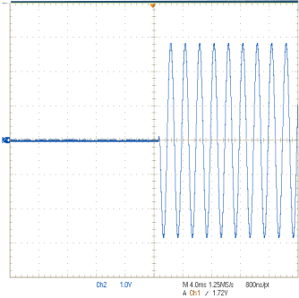 Figure 6. Mute to Play