SLOS681C January 2011 – August 2019 DRV632
PRODUCTION DATA.
- 1 Features
- 2 Applications
- 3 Description
- 4 Revision History
- 5 Device Comparison Table
- 6 Pin Configuration and Functions
- 7 Specifications
- 8 Parameter Measurement Information
- 9 Detailed Description
- 10Application and Implementation
- 11Power Supply Recommendations
- 12Layout
- 13Device and Documentation Support
- 14Mechanical, Packaging, and Orderable Information
Package Options
Mechanical Data (Package|Pins)
- PW|14
Thermal pad, mechanical data (Package|Pins)
Orderable Information
9.3.1 Line Driver Amplifiers
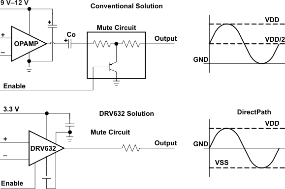
Single-supply line-driver amplifiers typically require dc-blocking capacitors. The top drawing in Figure 6 illustrates the conventional line-driver amplifier connection to the load and output signal. DC blocking capacitors are often large in value. The line load (typical resistive values of 600 Ω to 10 kΩ) combines with the dc blocking capacitors to form a high-pass filter. Equation 1 shows the relationship between the load impedance (RL), the capacitor (CO), and the cutoff frequency (fC).

CO can be determined using Equation 2, where the load impedance and the cutoff frequency are known.

If fC is low, the capacitor must then have a large value because the load resistance is small. Large capacitance values require large package sizes. Large package sizes consume PCB area, stand high above the PCB, increase cost of assembly, and can reduce the fidelity of the audio output signal.
 Figure 6. Conventional and DirectPath Line Drivers
 The DirectPath amplifier architecture operates from a single supply but makes use of an internal charge pump to provide a negative voltage rail. Combining the user-provided positive rail and the negative rail generated by the IC, the device operates in what is effectively a split-supply mode. The output voltages are now centered at zero volts with the capability to swing to the positive rail or negative rail. Combining this with the built-in click and pop reduction circuit, the DirectPath amplifier requires no output dc blocking capacitors. The bottom block diagram and waveform of Figure 6 illustrate the ground-referenced line-driver architecture. This is the architecture of the DRV632.