SLES256F May   2010  – May 2022 DRV8312 , DRV8332

PRODUCTION DATA  

  1. Features
  2. Applications
  3. Description
  4. Revision History
  5. Pin Configuration and Functions
  6. Specifications
    1. 6.1 Absolute Maximum Ratings
    2. 6.2 ESD Ratings
    3. 6.3 Recommended Operating Conditions
    4. 6.4 Thermal Information
    5. 6.5 Dissipation Ratings
    6. 6.6 Power Deratings (DRV8312)
    7. 6.7 Electrical Characteristics
    8. 6.8 Typical Characteristics
  7. Detailed Description
    1. 7.1 Overview
    2. 7.2 Functional Block Diagram
    3. 7.3 Feature Description
      1. 7.3.1 Error Reporting
      2. 7.3.2 Device Protection System
        1. 7.3.2.1 Bootstrap Capacitor Undervoltage Protection
          1. 7.3.2.1.1 Overcurrent (OC) Protection
        2. 7.3.2.2 Overtemperature Protection
        3. 7.3.2.3 Undervoltage Protection (UVP) and Power-On Reset (POR)
        4. 7.3.2.4 Device Reset
    4. 7.4 Device Functional Modes
      1. 7.4.1 Different Operational Modes
  8. Application and Implementation
    1. 8.1 Application Information
    2. 8.2 Typical Applications
      1. 8.2.1 Three-Phase Operation
        1. 8.2.1.1 Design Requirements
        2. 8.2.1.2 Detailed Design Procedure
          1. 8.2.1.2.1 Motor Voltage
          2. 8.2.1.2.2 Current Requirement of 12 V Power Supply
          3. 8.2.1.2.3 Voltage of Decoupling Capacitor
          4. 8.2.1.2.4 Overcurrent Threshold
          5. 8.2.1.2.5 Sense Resistor
          6. 8.2.1.2.6 Output Inductor Selection
        3. 8.2.1.3 Application Curves
      2. 8.2.2 DRV8312 Application Diagram for Three-Phase Operation
      3. 8.2.3 Control Signal Logic With Conventional 6 PWM Input Scheme
      4. 8.2.4 Hall Sensor Control With 6 Steps Trapezoidal Scheme
      5. 8.2.5 Sensorless Control With 6 Steps Trapezoidal Scheme
  9. Power Supply Recommendations
    1. 9.1 Bulk Capacitance
    2. 9.2 System Power-Up and Power-Down Sequence
      1. 9.2.1 Powering Up
      2. 9.2.2 Powering Down
    3. 9.3 System Design Recommendations
      1. 9.3.1 VREG Pin
      2. 9.3.2 VDD Pin
      3. 9.3.3 OTW Pin
      4. 9.3.4 FAULT Pin
      5. 9.3.5 OC_ADJ Pin
      6. 9.3.6 PWM_X and RESET_X Pins
      7. 9.3.7 Mode Select Pins
  10. 10Layout
    1. 10.1 Layout Guidelines
      1. 10.1.1 PCB Material Recommendation
      2. 10.1.2 Ground Plane
      3. 10.1.3 Decoupling Capacitor
      4. 10.1.4 AGND
    2. 10.2 Layout Example
      1. 10.2.1 Current Shunt Resistor
        1. 10.2.1.1 66
    3. 10.3 Thermal Considerations
      1. 10.3.1 Thermal Via Design Recommendation
  11. 11Device and Documentation Support
    1. 11.1 Related Links
    2. 11.2 Trademarks
    3. 11.3 Electrostatic Discharge Caution
    4. 11.4 Glossary
  12. 12Mechanical, Packaging, and Orderable Information

Package Options

Mechanical Data (Package|Pins)
Thermal pad, mechanical data (Package|Pins)
Orderable Information

Three-Phase Operation

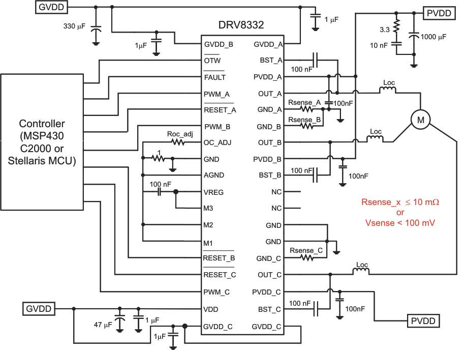
GUID-BAECA277-9B06-42BC-9718-AF2A0B5D3178-low.gifFigure 8-1 DRV8332 Application Diagram for Three-Phase Operation Schematic