SLRS063C September   2013  – February 2016 DRV8816

PRODUCTION DATA.  

  1. Features
  2. Applications
  3. Description
  4. Revision History
  5. Pin Configuration and Functions
  6. Specifications
    1. 6.1 Absolute Maximum Ratings
    2. 6.2 ESD Ratings
    3. 6.3 Recommended Operating Conditions
    4. 6.4 Thermal Information
    5. 6.5 Electrical Characteristics
    6. 6.6 Typical Characteristics
  7. Detailed Description
    1. 7.1 Overview
    2. 7.2 Functional Block Diagram
    3. 7.3 Feature Description
      1. 7.3.1 Bridge Control
      2. 7.3.2 Charge Pump
      3. 7.3.3 VPROPI
      4. 7.3.4 Protection Circuits
        1. 7.3.4.1 VBB UVLO
        2. 7.3.4.2 VCP UVLO (CPUV)
        3. 7.3.4.3 OCP
        4. 7.3.4.4 OTW
        5. 7.3.4.5 OTS
    4. 7.4 Device Functional Modes
      1. 7.4.1 SENSE
  8. Application and Implementation
    1. 8.1 Application Information
    2. 8.2 Typical Application
      1. 8.2.1 Design Requirements
      2. 8.2.2 Detailed Design Procedure
        1. 8.2.2.1 Motor Voltage
        2. 8.2.2.2 Power Dissipation
        3. 8.2.2.3 Motor Current Trip Point
        4. 8.2.2.4 Sense Resistor Selection
      3. 8.2.3 Application Curves
  9. Power Supply Recommendations
    1. 9.1 Bulk Capacitance
    2. 9.2 Power Supervisor
  10. 10Layout
    1. 10.1 Layout Guidelines
      1. 10.1.1 Ground
    2. 10.2 Layout Example
    3. 10.3 Thermal Protection
  11. 11Device and Documentation Support
    1. 11.1 Documentation Support
      1. 11.1.1 Related Documentation
    2. 11.2 Community Resource
    3. 11.3 Trademarks
    4. 11.4 Electrostatic Discharge Caution
    5. 11.5 Glossary
  12. 12Mechanical, Packaging, and Orderable Information

Package Options

Mechanical Data (Package|Pins)
Thermal pad, mechanical data (Package|Pins)
Orderable Information

5 Pin Configuration and Functions
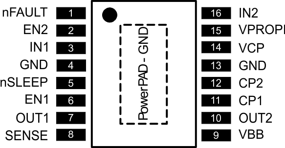
DRV8816 po_lrs063.gif

Pin Functions

PIN TYPE DESCRIPTION
NAME NO.
POWER AND GROUND
CP1 11 PWR Charge pump switching node Connect a 0.1-µF X7R capacitor rated for VBB between CP1 and CP2
CP2 12
GND 4, 13, PPAD PWR Device ground Connect to system ground
VBB 9 PWR Power supply input Connect to main power supply. Bypass to GND with a 0.1-µF ceramic capacitor and a larger bulk capacitor rated for at least the VBB voltage
VCP 14 PWR Charge pump output Connect a 0.1-µF 16-V ceramic capacitor between VCP and VBB
CONTROL
EN1 6 I ½-H bridge enable Logic high enables ½-H bridge output; logic low puts the FETs in HI-Z; internal pull-down
EN2 2
IN1 3 I ½-H bridge control Logic high enables the high-side ½-H bridge FET; logic low enables the low side FET; internal pull-down
IN2 16
nFAULT 1 O Fault indication pin Pulled logic low with fault condition; open-drain output requires an external pull-up. This output is indeterminate in sleep mode
nSLEEP 5 I Device sleep mode Pull logic low to put device into a low-power sleep mode; internal pull-down
OUTPUT
OUT1 7 O ½-H bridge output
OUT2 10 O ½-H bridge output
SENSE 8 O H-bridge low-side connect Connect directly to GND or through a sense resistor to set OCP
VPROPI
VPROPI 15 O Current-proportional output

Table 1. External Components

COMPONENT PIN 1 PIN 2 RECOMMENDED
CVBB VBB GND 0.1-µF ceramic capacitor and a larger bulk capacitor rated for at least the VBB voltage
CVCP VCP VBB 0.1-µF 16-V ceramic capacitor
RnFAULT VCC(1) nFAULT >1 kΩ resistor
RnSLEEP VCC(1) nSLEEP If nSLEEP isn't actively controlled, use a pull-up resistor of less than 20 kΩ
RSENSE SENSE GND Optional low-value resistor. If not used, connect SENSE pin directly to GND.
(1) VCC is not a pin on the DRV8816, but a VCC supply voltage pullup is required.