SLVSCP9 August 2014 DRV8833C
PRODUCTION DATA.
- 1 Features
- 2 Applications
- 3 Description
- 4 Revision History
- 5 Pin Configuration and Functions
- 6 Specifications
- 7 Detailed Description
- 8 Application and Implementation
- 9 Power Supply Recommendations
- 10Layout
- 11Device and Documentation Support
- 12Mechanical, Packaging, and Orderable Information
Package Options
Mechanical Data (Package|Pins)
Thermal pad, mechanical data (Package|Pins)
Orderable Information
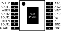
5 Pin Configuration and Functions
HTSSOP (PWP)
16 Pins
Top View
QFN (RTE)
16 Pins
Top View
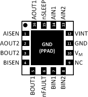
Pin Functions
| PIN | TYPE | DESCRIPTION | |||
|---|---|---|---|---|---|
| NAME | PWP | RTE | |||
| POWER AND GROUND | |||||
| GND | 13 | 11 | PWR | Device ground | Both the GND pin and device PowerPAD must be connected to ground |
| VINT | 14 | 12 | — | Internal regulator (3.3 V) | Internal supply voltage; bypass to GND with 2.2-μF, 6.3-V capacitor |
| VM | 12 | 10 | PWR | Power supply | Connect to motor supply voltage; bypass to GND with a 10-µF (minimum) capacitor rated for VM |
| CONTROL | |||||
| AIN1 | 16 | 14 | I | H-bridge A PWM input | Controls the state of AOUT1 and AOUT2; internal pulldown |
| AIN2 | 15 | 13 | |||
| BIN1 | 9 | 7 | I | H-bridge B PWM input | Controls the state of BOUT1 and BOUT2; internal pulldown |
| BIN2 | 10 | 8 | |||
| nSLEEP | 1 | 15 | I | Sleep mode input | Logic high to enable device; logic low to enter low-power sleep mode; internal pulldown |
| STATUS | |||||
| nFAULT | 8 | 6 | OD | Fault indication pin | Pulled logic low with fault condition; open-drain output requires an external pullup |
| OUTPUT | |||||
| AISEN | 3 | 1 | O | Bridge A sense | Sense resistor to GND sets PWM current regulation level (seePWM Motor Drivers) |
| AOUT1 | 2 | 16 | O | Bridge A output | Positive current is AOUT1 → AOUT2 |
| AOUT2 | 4 | 2 | |||
| BISEN | 6 | 4 | O | Bridge B sense | Sense resistor to GND sets PWM current regulation level (see PWM Motor Drivers) |
| BOUT1 | 7 | 5 | O | Bridge B output | Positive current is BOUT1 → BOUT2 |
| BOUT2 | 5 | 3 | |||
External Components
| Component | Pin 1 | Pin 2 | Recommended |
|---|---|---|---|
| CVM | VM | GND | 10-µF(2) ceramic capacitor rated for VM |
| CVINT | VINT | GND | 6.3-V, 2.2-µF ceramic capacitor |
| RnFAULT | VINT(1) | nFAULT | >1 kΩ |
| RAISEN | AISEN | GND | Sense resistor, see Typical Application for sizing |
| RBISEN | BISEN | GND | Sense resistor, see Typical Application for sizing |
(1) nFAULT may be pulled up to an external supply rated < 5.5 V.
(2) Proper bulk capacitance sizing depends on the motor power.