SLVSB18H March 2012 – August 2016 DRV8835
PRODUCTION DATA.
- 1 Features
- 2 Applications
- 3 Description
- 4 Revision History
- 5 Pin Configuration and Functions
- 6 Specifications
- 7 Detailed Description
- 8 Application and Implementation
- 9 Power Supply Recommendations
- 10Layout
- 11Device and Documentation Support
- 12Mechanical, Packaging, and Orderable Information
Package Options
Mechanical Data (Package|Pins)
- DSS|12
Thermal pad, mechanical data (Package|Pins)
- DSS|12
Orderable Information
10 Layout
10.1 Layout Guidelines
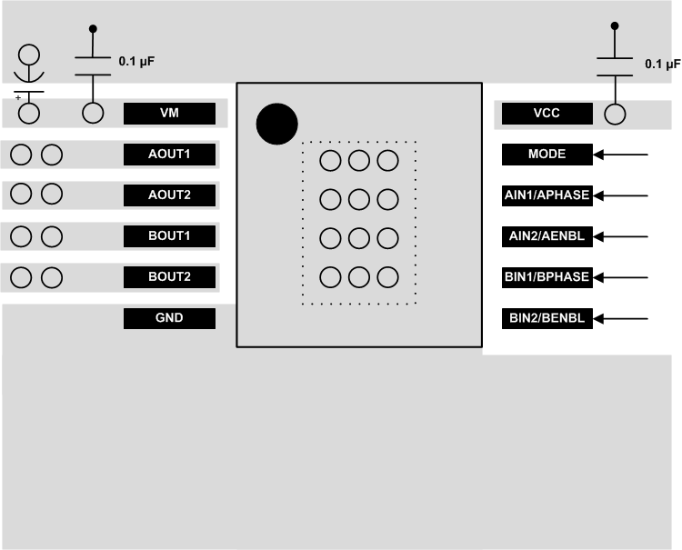
The VCC pin should be bypassed to GND using low-ESR ceramic bypass capacitors with a recommended value of 0.1 μF rated for VCC. This capacitor should be placed as close to the VCC pin as possible with a thick trace.
The VM pin should be bypassed to GND using low-ESR ceramic bypass capacitors with a recommended value of 0.1 μF rated for VM. This capacitor should be placed as close to the VM pin as possible with a thick trace. The VM pin must bypass to ground using an appropriate bulk capacitor. This component can be an electrolytic and should be located close to the DRV8835.
10.3 Thermal Considerations
The DRV8835 has thermal shutdown (TSD) as described above. If the die temperature exceeds approximately 150°C, the device disables until the temperature drops to a safe level.
Any tendency of the device to enter thermal shutdown is an indication of either excessive power dissipation, insufficient heatsinking, or excessively high ambient temperature.
10.3.1 Power Dissipation
Power dissipation in the DRV8835 is dominated by the power dissipated in the output FET resistance, or RDS(on). Average power dissipation when running both H-bridges can be roughly estimated by Equation 1:
where
- PTOT is the total power dissipation, RDS(ON) is the resistance of the HS plus LS FETs, and IOUT(RMS) is the RMS output current being applied to each winding. IOUT(RMS) is equal to the approximately 0.7× the full-scale output current setting. The factor of 2 comes from the fact that there are two H-bridges.
The maximum amount of power dissipated in the device is dependent on ambient temperature and heatsinking.
NOTE
RDS(on) increases with temperature, so as the device heats, the power dissipation increases. Consider this increase when sizing the heatsink.
The power dissipation of the DRV8835 is a function of RMS motor current and the resistance of each FET (RDS(ON)), see Equation 2.
For this example, the ambient temperature is 35°C, and the junction temperature reaches 65°C. At 65°C, the sum of RDS(on) is about 1 Ω. With an example motor current of 0.8 A, the dissipated power in the form of heat will be 0.8 A2 × 1 Ω = 0.64 W.
The temperature that the DRV8835 reaches depends on the thermal resistance to the air and PCB. It is important to solder the device thermal pad to the PCB ground plane, with vias to the top and bottom board layers, in order dissipate heat into the PCB and reduce the device temperature. In the example used here, the DRV8835 had an effective thermal resistance RθJA of 47°C/W, and as shown in Equation 3.
10.3.2 Heatsinking
The package uses an exposed pad to remove heat from the device. For proper operation, this pad must thermally connect to copper on the PCB to dissipate heat. On a multi-layer PCB with a ground plane, this can be accomplished by adding a number of vias to connect the thermal pad to the ground plane. On PCBs without internal planes, copper area can be added on either side of the PCB to dissipate heat. If the copper area is on the opposite side of the PCB from the device, thermal vias are used to transfer the heat between top and bottom layers.
For more PCB design details, refer to QFN/SON PCB Attachment and AN-1187 Leadless Leadframe Package (LLP), available at www.ti.com.
In general, the more copper area that is provided, the more power can be dissipated.
