SLVSBA4F June 2012 – April 2021 DRV8837 , DRV8838
PRODUCTION DATA
- 1 Features
- 2 Applications
- 3 Description
- 4 Revision History
- 5 Pin Configuration and Functions
- 6 Specifications
- 7 Detailed Description
- 8 Power Supply Recommendations
- 9 Layout
- 10Device and Documentation Support
Package Options
Mechanical Data (Package|Pins)
- DSG|8
Thermal pad, mechanical data (Package|Pins)
- DSG|8
Orderable Information
3 Description
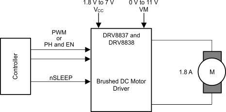
The DRV883x family of devices provides an integrated motor driver solution for cameras, consumer products, toys, and other low-voltage or battery-powered motion control applications. The device can drive one dc motor or other devices like solenoids. The output driver block consists of N-channel power MOSFETs configured as an H-bridge to drive the motor winding. An internal charge pump generates needed gate drive voltages.
The DRV883x family of devices can
supply up to
1.8 A of output current. It operates on a
motor power supply voltage from 0 to 11 V, and a device power supply voltage of 1.8
V to 7 V.
The DRV8837 device has a PWM (IN1-IN2) input interface; the DRV8838 device has a PH-EN input interface. Both interfaces are compatible with industry-standard devices.
Internal shutdown functions are provided for overcurrent protection, short-circuit protection, undervoltage lockout, and overtemperature.
| PART NUMBER | PACKAGE | BODY SIZE (NOM) |
|---|---|---|
| DRV8837 | WSON (8) | 2.00 mm × 2.00 mm |
| DRV8838 |
 DRV883x Simplified Diagram