SLVSCY9B August   2015  – July 2016 DRV8871

PRODUCTION DATA.  

  1. Features
  2. Applications
  3. Description
    1.     Device Images
      1.      Simplified Schematic
      2.      Peak Current Regulation
  4. Revision History
  5. Pin Configuration and Functions
    1.     Pin Functions
  6. Specifications
    1. 6.1 Absolute Maximum Ratings
    2. 6.2 ESD Ratings
    3. 6.3 Recommended Operating Conditions
    4. 6.4 Thermal Information
    5. 6.5 Electrical Characteristics
    6. 6.6 Typical Characteristics
  7. Detailed Description
    1. 7.1 Overview
    2. 7.2 Functional Block Diagram
    3. 7.3 Feature Description
      1. 7.3.1 Bridge Control
      2. 7.3.2 Sleep Mode
      3. 7.3.3 Current Regulation
      4. 7.3.4 Dead Time
      5. 7.3.5 Protection Circuits
        1. 7.3.5.1 VM Undervoltage Lockout (UVLO)
        2. 7.3.5.2 Overcurrent Protection (OCP)
        3. 7.3.5.3 Thermal Shutdown (TSD)
    4. 7.4 Device Functional Modes
      1. 7.4.1 PWM With Current Regulation
      2. 7.4.2 PWM Without Current Regulation
      3. 7.4.3 Static Inputs With Current Regulation
      4. 7.4.4 VM Control
  8. Application and Implementation
    1. 8.1 Application Information
    2. 8.2 Typical Application
      1. 8.2.1 Design Requirements
      2. 8.2.2 Detailed Design Procedure
        1. 8.2.2.1 Motor Voltage
        2. 8.2.2.2 Drive Current
      3. 8.2.3 Application Curves
  9. Power Supply Recommendations
    1. 9.1 Bulk Capacitance
  10. 10Layout
    1. 10.1 Layout Guidelines
    2. 10.2 Layout Example
    3. 10.3 Thermal Considerations
    4. 10.4 Power Dissipation
      1. 10.4.1 Heatsinking
  11. 11Device and Documentation Support
    1. 11.1 Documentation Support
      1. 11.1.1 Related Documentation
    2. 11.2 Receiving Notification of Documentation Updates
    3. 11.3 Community Resources
    4. 11.4 Trademarks
    5. 11.5 Electrostatic Discharge Caution
    6. 11.6 Glossary
  12. 12Mechanical, Packaging, and Orderable Information

Package Options

Refer to the PDF data sheet for device specific package drawings

Mechanical Data (Package|Pins)
  • DDA|8
Thermal pad, mechanical data (Package|Pins)
Orderable Information

Current Regulation

The DRV8871 device limits the output current based on a standard resistor attached to pin ILIM, according to this equation:

Equation 1. DRV8871 eq_I_TRIP_lvscy9.gif

For example, if RILIM = 32 kΩ, the DRV8871 device limits motor current to 2 A no matter how much load torque is applied. The minimum allowed RILIM is 15 kΩ. System designers should always understand the min and max ITRIP, based on the RILIM resistor component tolerance and the DRV8871 specified VILIM range.

When ITRIP has been reached, the device enforces slow current decay by enabling both low-side FETs, and it does this for time tOFF (typically 25 µs).
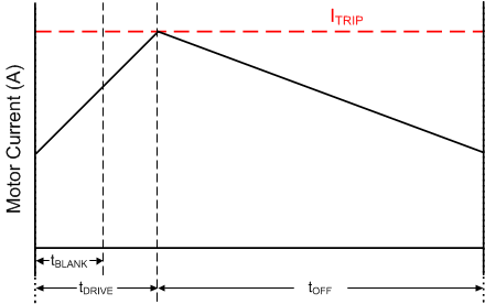
DRV8871 current_reg_lvscy9.gifFigure 5. Current Regulation Time Periods

After tOFF has elapsed, the output is re-enabled according to the two inputs INx. The drive time (tDRIVE) until reaching another ITRIP event heavily depends on the VM voltage, the motor’s back-EMF, and the motor’s inductance.