SLVSF67B August   2019  – January 2021 DRV8874-Q1

PRODUCTION DATA  

  1. Features
  2. Applications
  3. Description
  4. Revision History
  5. Pin Configuration and Functions
    1.     Pin Functions
  6. Specifications
    1. 6.1 Absolute Maximum Ratings
    2. 6.2 ESD Ratings
    3. 6.3 Recommended Operating Conditions
    4. 6.4 Thermal Information
    5. 6.5 Electrical Characteristics
    6. 6.6 Typical Characteristics
  7. Detailed Description
    1. 7.1 Overview
    2. 7.2 Functional Block Diagram
    3. 7.3 Feature Description
      1. 7.3.1 External Components
      2. 7.3.2 Control Modes
        1. 7.3.2.1 PH/EN Control Mode (PMODE = Logic Low)
        2. 7.3.2.2 PWM Control Mode (PMODE = Logic High)
        3. 7.3.2.3 Independent Half-Bridge Control Mode (PMODE = Hi-Z)
      3. 7.3.3 Current Sense and Regulation
        1. 7.3.3.1 Current Sensing
        2. 7.3.3.2 Current Regulation
          1. 7.3.3.2.1 Fixed Off-Time Current Chopping
          2. 7.3.3.2.2 Cycle-By-Cycle Current Chopping
      4. 7.3.4 Protection Circuits
        1. 7.3.4.1 VM Supply Undervoltage Lockout (UVLO)
        2. 7.3.4.2 VCP Charge Pump Undervoltage Lockout (CPUV)
        3. 7.3.4.3 OUTx Overcurrent Protection (OCP)
        4. 7.3.4.4 Thermal Shutdown (TSD)
        5. 7.3.4.5 Fault Condition Summary
      5. 7.3.5 Pin Diagrams
        1. 7.3.5.1 Logic-Level Inputs
        2. 7.3.5.2 Tri-Level Inputs
        3. 7.3.5.3 Quad-Level Inputs
    4. 7.4 Device Functional Modes
      1. 7.4.1 Active Mode
      2. 7.4.2 Low-Power Sleep Mode
      3. 7.4.3 Fault Mode
  8. Application and Implementation
    1. 8.1 Application Information
    2. 8.2 Typical Application
      1. 8.2.1 Primary Application
        1. 8.2.1.1 Design Requirements
        2. 8.2.1.2 Detailed Design Procedure
          1. 8.2.1.2.1 Current Sense and Regulation
          2. 8.2.1.2.2 Power Dissipation and Output Current Capability
          3. 8.2.1.2.3 Thermal Performance
            1. 8.2.1.2.3.1 Steady-State Thermal Performance
            2. 8.2.1.2.3.2 Transient Thermal Performance
        3. 8.2.1.3 Application Curves
      2. 8.2.2 Alternative Application
        1. 8.2.2.1 Design Requirements
        2. 8.2.2.2 Detailed Design Procedure
          1. 8.2.2.2.1 Current Sense and Regulation
        3. 8.2.2.3 Application Curves
  9. Power Supply Recommendations
    1. 9.1 Bulk Capacitance
  10. 10Layout
    1. 10.1 Layout Guidelines
    2. 10.2 Layout Example
      1. 10.2.1 HTSSOP Layout Example
  11. 11Device and Documentation Support
    1. 11.1 Documentation Support
      1. 11.1.1 Related Documentation
    2. 11.2 Receiving Notification of Documentation Updates
    3. 11.3 Community Resources
    4. 11.4 Trademarks
  12. 12Mechanical, Packaging, and Orderable Information

Package Options

Mechanical Data (Package|Pins)
Thermal pad, mechanical data (Package|Pins)
Orderable Information
Steady-State Thermal Performance

"Steady-state" conditions assume that the motor driver operates with a constant RMS current over a long period of time. Figure 8-3, Figure 8-4, Figure 8-5, and Figure 8-6 show how RθJA and ΨJB (junction-to-board characterization parameter) change depending on copper area, copper thickness, and number of layers of the PCB for the HTSSOP package. More copper area, more layers, and thicker copper planes decrease RθJA and ΨJB, which indicate better thermal performance from the PCB layout.
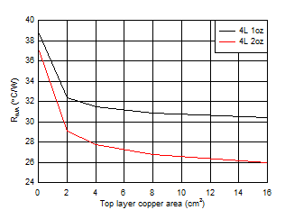
GUID-67CE533C-1673-4750-BEDE-FC2B8C7E386E-low.gifFigure 8-3 HTSSOP, 4-layer PCB junction-to-ambient thermal resistance vs copper area
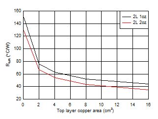
GUID-1BA49CC3-9E53-41FC-AEFC-53183BC51E67-low.gifFigure 8-5 HTSSOP, 2-layer PCB junction-to-ambient thermal resistance vs copper area
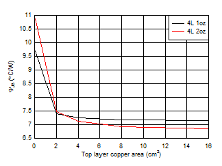
GUID-68339F61-50A5-46FF-ACD5-B1CC4135FCB5-low.gifFigure 8-4 HTSSOP, 4-layer PCB junction-to-board characterization parameter vs copper area
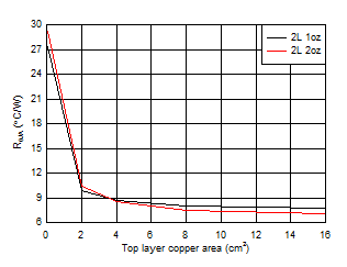
GUID-42C1E96C-158F-4A3D-A735-699D5C79A24D-low.gifFigure 8-6 HTSSOP, 2-layer PCB junction-to-board characterization parameter vs copper area