SLVSF66A August   2019  – December  2019 DRV8874

PRODUCTION DATA.  

  1. Features
  2. Applications
  3. Description
    1.     Device Images
      1.      Simplified Schematic
  4. Revision History
  5. Pin Configuration and Functions
    1.     Pin Functions
  6. Specifications
    1. 6.1 Absolute Maximum Ratings
    2. 6.2 ESD Ratings
    3. 6.3 Recommended Operating Conditions
    4. 6.4 Thermal Information
    5. 6.5 Electrical Characteristics
    6. 6.6 Typical Characteristics
  7. Detailed Description
    1. 7.1 Overview
    2. 7.2 Functional Block Diagram
    3. 7.3 Feature Description
      1. 7.3.1 External Components
      2. 7.3.2 Control Modes
        1. 7.3.2.1 PH/EN Control Mode (PMODE = Logic Low)
        2. 7.3.2.2 PWM Control Mode (PMODE = Logic High)
        3. 7.3.2.3 Independent Half-Bridge Control Mode (PMODE = Hi-Z)
      3. 7.3.3 Current Sense and Regulation
        1. 7.3.3.1 Current Sensing
        2. 7.3.3.2 Current Regulation
          1. 7.3.3.2.1 Fixed Off-Time Current Chopping
          2. 7.3.3.2.2 Cycle-By-Cycle Current Chopping
      4. 7.3.4 Protection Circuits
        1. 7.3.4.1 VM Supply Undervoltage Lockout (UVLO)
        2. 7.3.4.2 VCP Charge Pump Undervoltage Lockout (CPUV)
        3. 7.3.4.3 OUTx Overcurrent Protection (OCP)
        4. 7.3.4.4 Thermal Shutdown (TSD)
        5. 7.3.4.5 Fault Condition Summary
      5. 7.3.5 Pin Diagrams
        1. 7.3.5.1 Logic-Level Inputs
        2. 7.3.5.2 Tri-Level Inputs
        3. 7.3.5.3 Quad-Level Inputs
    4. 7.4 Device Functional Modes
      1. 7.4.1 Active Mode
      2. 7.4.2 Low-Power Sleep Mode
      3. 7.4.3 Fault Mode
  8. Application and Implementation
    1. 8.1 Application Information
    2. 8.2 Typical Application
      1. 8.2.1 Primary Application
        1. 8.2.1.1 Design Requirements
        2. 8.2.1.2 Detailed Design Procedure
          1. 8.2.1.2.1 Current Sense and Regulation
          2. 8.2.1.2.2 Power Dissipation and Output Current Capability
          3. 8.2.1.2.3 Thermal Performance
            1. 8.2.1.2.3.1 Steady-State Thermal Performance
            2. 8.2.1.2.3.2 Transient Thermal Performance
        3. 8.2.1.3 Application Curves
      2. 8.2.2 Alternative Application
        1. 8.2.2.1 Design Requirements
        2. 8.2.2.2 Detailed Design Procedure
          1. 8.2.2.2.1 Current Sense and Regulation
        3. 8.2.2.3 Application Curves
  9. Power Supply Recommendations
    1. 9.1 Bulk Capacitance
  10. 10Layout
    1. 10.1 Layout Guidelines
    2. 10.2 Layout Example
      1. 10.2.1 HTSSOP Layout Example
  11. 11Device and Documentation Support
    1. 11.1 Documentation Support
      1. 11.1.1 Related Documentation
    2. 11.2 Receiving Notification of Documentation Updates
    3. 11.3 Community Resources
    4. 11.4 Trademarks
    5. 11.5 Electrostatic Discharge Caution
    6. 11.6 Glossary
  12. 12Mechanical, Packaging, and Orderable Information

Package Options

Mechanical Data (Package|Pins)
Thermal pad, mechanical data (Package|Pins)
Orderable Information

Application Curves

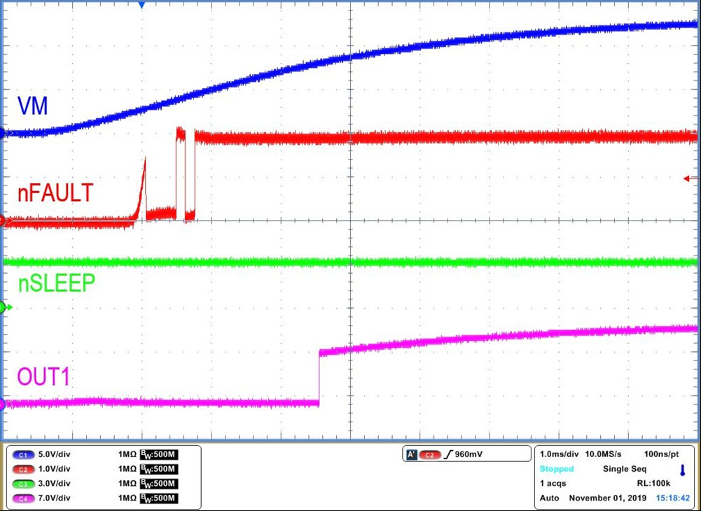
DRV8874 slvsds7-thebe-pwr-up.png
Chan. 1 = VM Chan. 2 = nFAULT Chan. 3 = nSLEEP
Chan. 4 = IOUT
Figure 27. Device Power-up with Supply Voltage (VM) Ramp
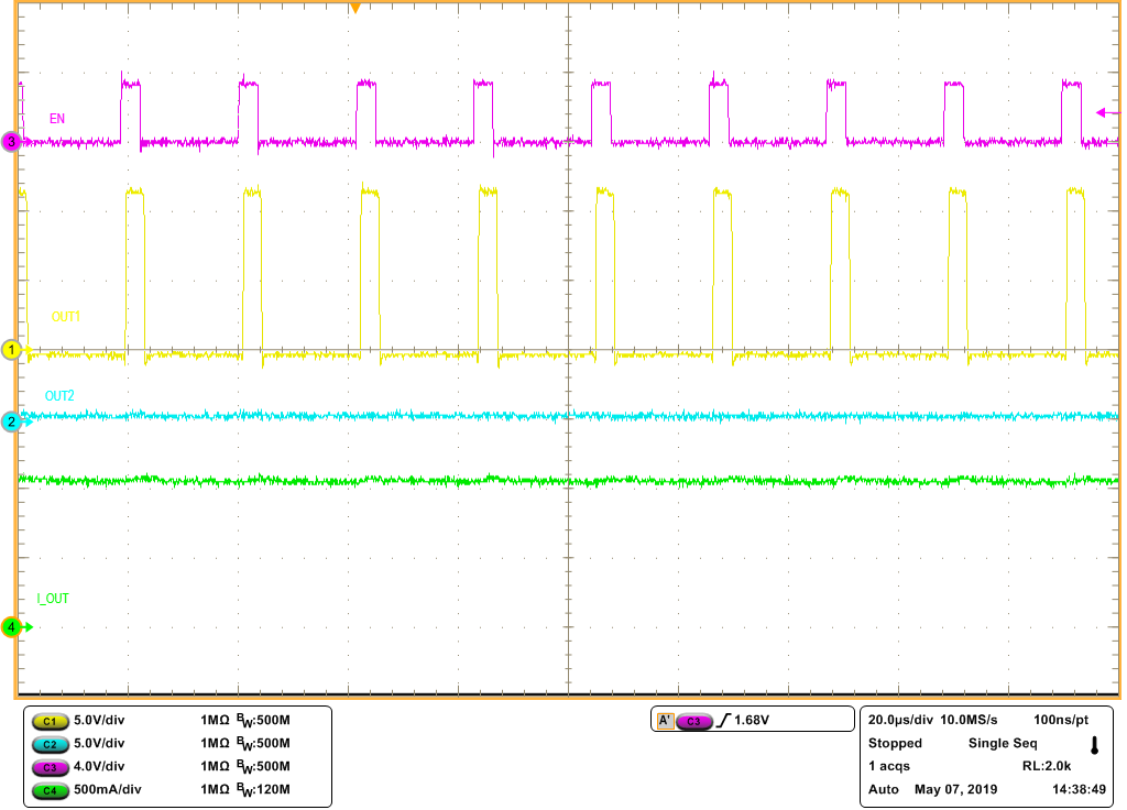
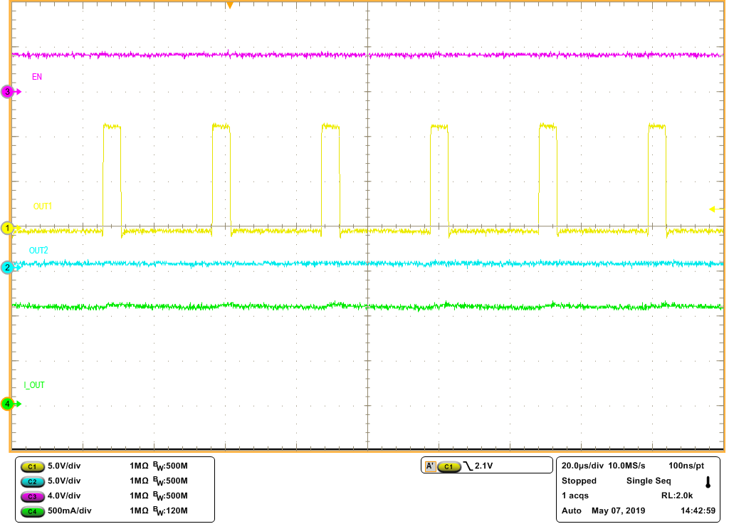
DRV8874 normal_operation.png
Chan. 1 = OUT1 Chan. 2 = OUT2 Chan. 3 = EN/IN1
Chan. 4 = IOUT
Figure 29. Driver PWM Operation (PH/EN)
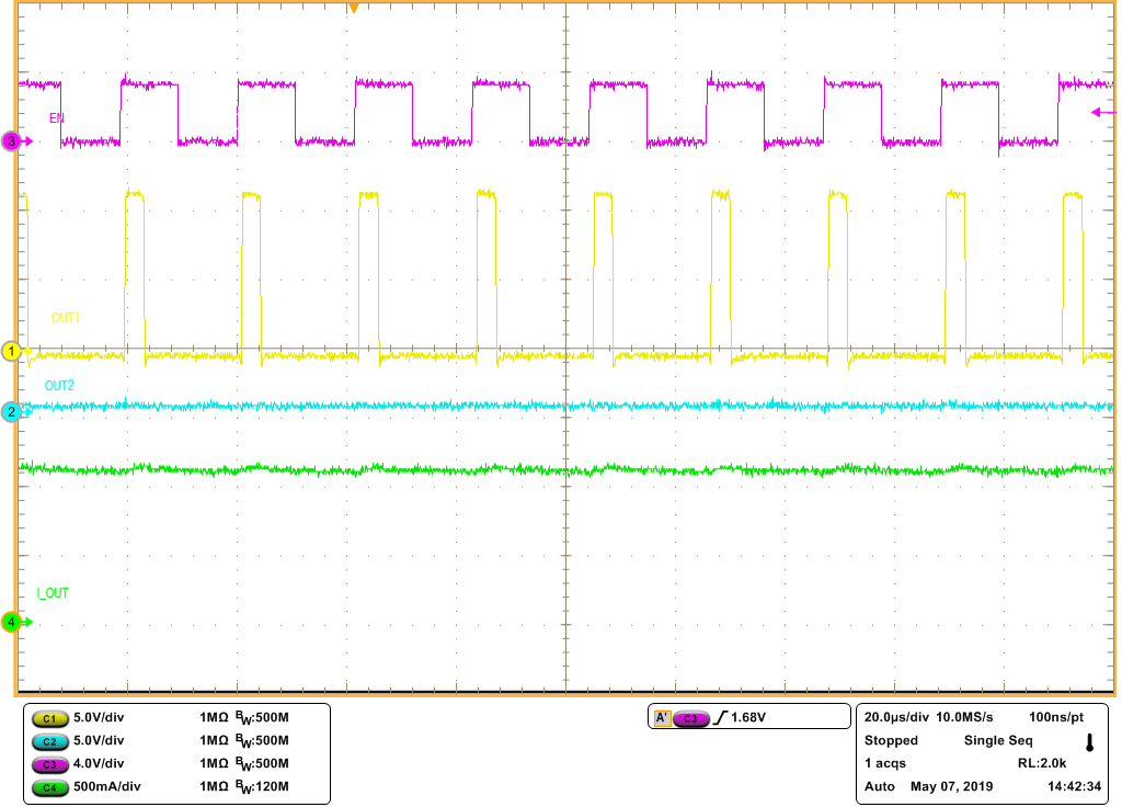
DRV8874 normal chop w pwm.png
Chan. 1 = OUT1 Chan. 2 = OUT2 Chan. 3 = EN/IN1
Chan. 4 = IOUT
Figure 31. Driver PWM Operation With Current Chopping
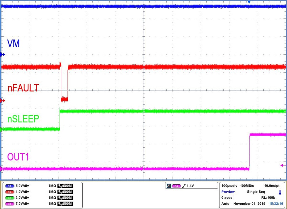
DRV8874 slvsds7-thebe-slp.png
Chan. 1 = VM Chan. 2 = nFAULT Chan. 3 = nSLEEP
Chan. 4 = IOUT
Figure 28. Device Power-up with nSLEEP
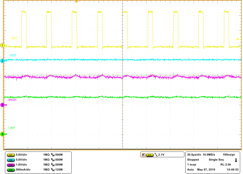
DRV8874 normal w ipropi.png
Chan. 1 = OUT1 Chan. 2 = OUT2 Chan. 3 = IPROPI
Chan. 4 = IOUT
Figure 30. Driver PWM Operation With Current Feedback
DRV8874 normal chop wo pwm.png
Chan. 1 = OUT1 Chan. 2 = OUT2 Chan. 3 = EN/IN1
Chan. 4 = IOUT
Figure 32. Driver Full On Operation With Current Chopping