SLVSDA4C January 2017 – March 2020 DRV8886
PRODUCTION DATA.
- 1 Features
- 2 Applications
- 3 Description
- 4 Revision History
- 5 Pin Configuration and Functions
- 6 Specifications
-
7 Detailed Description
- 7.1 Overview
- 7.2 Functional Block Diagram
- 7.3
Feature Description
- 7.3.1 Stepper Motor Driver Current Ratings
- 7.3.2 PWM Motor Drivers
- 7.3.3 Microstepping Indexer
- 7.3.4 Current Regulation
- 7.3.5 Controlling RREF With an MCU DAC
- 7.3.6 Decay Modes
- 7.3.7 Blanking Time
- 7.3.8 Charge Pump
- 7.3.9 Linear Voltage Regulators
- 7.3.10 Logic and Multi-Level Pin Diagrams
- 7.3.11 Protection Circuits
- 7.4 Device Functional Modes
- 8 Application and Implementation
- 9 Power Supply Recommendations
- 10Layout
- 11Device and Documentation Support
- 12Mechanical, Packaging, and Orderable Information
Package Options
Mechanical Data (Package|Pins)
Thermal pad, mechanical data (Package|Pins)
Orderable Information
7.3.4 Current Regulation
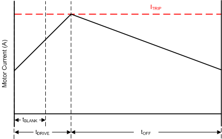
The current through the motor windings is regulated by an adjustable, fixed-off-time PWM current-regulation circuit. When an H-bridge is enabled, current rises through the winding at a rate dependent on the supply voltage, inductance of the winding, and the magnitude of the back EMF present. When the current hits the current regulation threshold, the bridge enters a decay mode for a fixed 20 μs, period of time to decrease the current. After the off time expires, the bridge is re-enabled, starting another PWM cycle.
 Figure 14. Current Chopping Waveform
 The PWM regulation current is set by a comparator which monitors the voltage across the current sense MOSFETs in parallel with the low-side power MOSFETs. The current sense MOSFETs are biased with a reference current that is the output of a current-mode sine-weighted DAC whose full-scale reference current is set by the current through the RREF pin. An external resistor is placed from the RREF pin to GND to set the reference current. In addition, the TRQ pin can further scale the reference current.
Use Equation 1 to calculate the full-scale regulation current.

For example, if a 30-kΩ resistor is connected to the RREF pin, the full-scale regulation current is 1 A (TRQ at 100%).
The TRQ pin is the input to a DAC used to scale the output current. Table 5 lists the current scalar value for different inputs.
Table 5. Torque DAC Settings
| TRQ | CURRENT SCALAR (TRQ) |
|---|---|
| 0 | 100% |
| Z | 75% |
| 1 | 50% |