SLOSE58B May 2020 – May 2022 DRV8932
PRODUCTION DATA
- 1 Features
- 2 Applications
- 3 Description
- 4 Revision History
- 5 Pin Configuration and Functions
- 6 Specifications
- 7 Detailed Description
- 8 Application and Implementation
- 9 Power Supply Recommendations
- 10Layout
- 11Device and Documentation Support
- 12Mechanical, Packaging, and Orderable Information
Package Options
Mechanical Data (Package|Pins)
Thermal pad, mechanical data (Package|Pins)
- RGE|24
Orderable Information
7.3.2 Current Regulation
When an output load is connected to the VM supply, the load current can be regulated to the ITRIP level. The ITRIP current level for OUT1 and OUT2 outputs is controlled by the VREF12 pin, and the ITRIP level for OUT3 and OUT4 outputs is controlled by the VREF34 pin. The ITRIP current (ITRIP) can be calculated as ITRIP (A) = VREF (V) / 2.2 (V/A). The VREF voltage can be programmed by connecting resistor dividers from DVDD pin to ground. Both VREF pins can be tied together to program the same ITRIP current for all four output channels.
The DRV8932 can simultaneously drive four resistive or inductive loads connected to VM supply. With INx = 0, the low side FET is turned ON till the current increases and hits the ITRIP level. Once the load current equals ITRIP, the low-side FET is turned OFF and the high-side FET is turned on for a period of off-time determined by the TOFF pin. After the off-time expires, the low-side FET is again turned ON and the cycle repeats. The OFF time settings can be changed on the fly. After a OFF time setting change, the new OFF time is applied after a 10 µs de-glitch time.
For resistive loads connected to VM, if the ITRIP is higher than the (VM / RLOAD), the load current is regulated at VM / RLOAD level while INx = 0. For inductive loads connected to VM, it should be ensured that the current decays enough every cycle to prevent runaway and triggering overcurrent protection. The different scenarios are shown below -
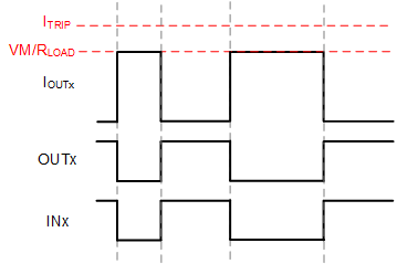 Figure 7-3 Resistive Load Connected to VM, Cycle-by-cycle control, ITRIP is higher than VM/RLOAD.
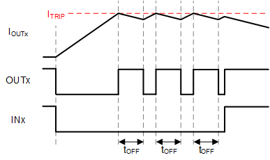 Figure 7-4 Inductive Load Connected to VM, fixed off-time current chopping
Another way of controlling the load current is the cycle-by-cycle control mode, where PWM pulse width of the INx input pins are controlled. This allows for additional control of the current chopping scheme by the external controller. For loads connected to VM, when INx = 0, the current through the load builds up; and when INx = 1, the current through the load decays. By properly choosing the duty cycle of the INx pulse, current can be regulated to a target value. Various such scenarios are shown below -
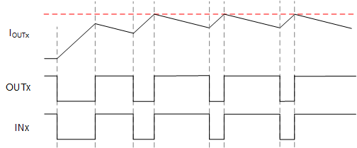 Figure 7-5 Inductive Load Connected to VM, Cycle-by-cycle control
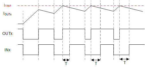 Figure 7-6 Inductive Load Connected to VM, Cycle-by-cycle control, T has to be less than TOFF of the DRV8932.
Similarly, current through loads connected to ground can be controlled by controlling the INx pin pulse width - INx = 1 builds up the current, and INx = 0 decays the current. Two such scenarios are shown below -
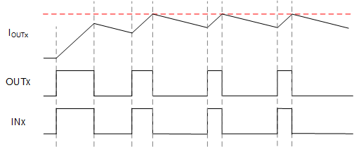 Figure 7-7 Inductive Load Connected to ground, Cycle-by-cycle control.
 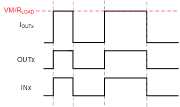 Figure 7-8 Resistive Load Connected to ground, Cycle-by-cycle control.
 | TOFF | OFF-TIME tOFF |
|---|---|
| 0 | 7 µs |
| 1 | 16 µs |
| Hi-Z | 24 µs |
| 330kΩ to GND | 32 µs |