SLOSE71 April   2020  – December 2020 DRV8955

PRODUCTION DATA  

  1. Features
  2. Applications
  3. Description
  4. Revision History
  5. Pin Configuration and Functions
    1.     Pin Functions
  6. Specifications
    1. 6.1 Absolute Maximum Ratings
    2. 6.2 ESD Ratings
    3. 6.3 Recommended Operating Conditions
    4. 6.4 Thermal Information
    5. 6.5 Electrical Characteristics
      1. 6.5.1 Typical Characteristics
  7. Detailed Description
    1. 7.1 Overview
    2. 7.2 Functional Block Diagrams
    3. 7.3 Feature Description
      1. 7.3.1 Configuration Options and Bridge Control
      2. 7.3.2 Current Regulation
      3. 7.3.3 Charge Pump
      4. 7.3.4 Linear Voltage Regulators
      5. 7.3.5 Logic and Quad-Level Pin Diagrams
        1. 7.3.5.1 nFAULT Pin
      6. 7.3.6 Protection Circuits
        1. 7.3.6.1 VM Undervoltage Lockout (UVLO)
        2. 7.3.6.2 VCP Undervoltage Lockout (CPUV)
        3. 7.3.6.3 Overcurrent Protection (OCP)
        4. 7.3.6.4 Thermal Shutdown (OTSD)
        5.       Fault Condition Summary
    4. 7.4 Device Functional Modes
      1. 7.4.1 Sleep Mode (nSLEEP = 0)
      2. 7.4.2 Operating Mode (nSLEEP = 1)
      3. 7.4.3 nSLEEP Reset Pulse
      4.      Functional Modes Summary
  8. Application and Implementation
    1. 8.1 Application Information
    2. 8.2 Typical Application
      1. 8.2.1 Design Requirements
      2. 8.2.2 Detailed Design Procedure
        1. 8.2.2.1 Current Regulation
        2. 8.2.2.2 Power Dissipation and Thermal Calculation
        3. 8.2.2.3 Application Curves
  9. Power Supply Recommendations
    1. 9.1 Bulk Capacitance Sizing
  10. 10Layout
    1. 10.1 Layout Guidelines
    2. 10.2 Layout Example
  11. 11Device and Documentation Support
    1. 11.1 Documentation Support
      1. 11.1.1 Related Documentation
    2. 11.2 Receiving Notification of Documentation Updates
    3. 11.3 Support Resources
    4. 11.4 Trademarks
    5. 11.5 Electrostatic Discharge Caution
    6. 11.6 Glossary
  12. 12Mechanical, Packaging, and Orderable Information

Package Options

Mechanical Data (Package|Pins)
Thermal pad, mechanical data (Package|Pins)
Orderable Information

Typical Characteristics

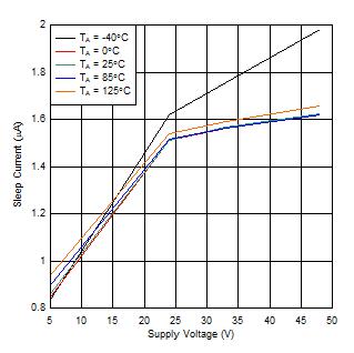
GUID-6C3D59AA-D3DB-4A92-BF41-55FA6B43A85C-low.jpgFigure 6-1 Sleep Current over Supply Voltage
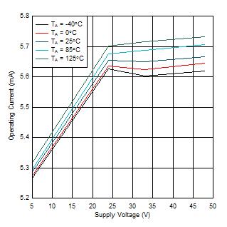
GUID-EE61F277-07ED-42F6-9FAD-D6BB4865AF61-low.jpgFigure 6-3 Operating Current over Supply Voltage
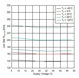
GUID-1EDE0284-D78D-456B-8A44-4E482AB5986B-low.jpgFigure 6-5 Low-Side RDS(ON) over Supply Voltage (MODE = 0 or 330k to GND)
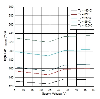
GUID-1A4416C8-C7AF-40CC-BAC0-BB97AE7D3B14-low.jpgFigure 6-7 High-Side RDS(ON) over Supply Voltage (MODE = 0 or 330k to GND)
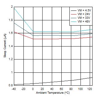
GUID-DCDD2A57-99DC-4D8E-8A32-76BCFF2A61FA-low.jpgFigure 6-2 Sleep Current over Temperature
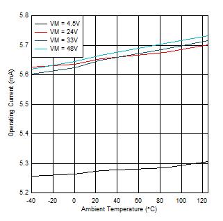
GUID-A24F5AEE-367F-4580-8D52-509A6D055329-low.jpgFigure 6-4 Operating Current over Temperature
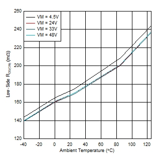
GUID-81187239-1A46-42FF-B842-2F14DD06E96B-low.jpgFigure 6-6 Low-Side RDS(ON) over Temperature (MODE = 0 or 330k to GND)
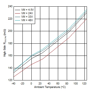
GUID-D795B573-B825-489C-978C-195E125733A3-low.jpgFigure 6-8 High-Side RDS(ON) over Temperature (MODE = 0 or 330k to GND)