SNLS450A January 2014 – June 2015 DS125DF111
PRODUCTION DATA.
- 1 Features
- 2 Applications
- 3 Description
- 4 Revision History
- 5 Pin Configuration And Functions
- 6 Specifications
-
7 Detailed Description
- 7.1 Overview
- 7.2 Functional Block Diagram
- 7.3 Feature Description
- 7.4 Device Functional Modes
- 7.5
Programming
- 7.5.1
SMBus Interface
- 7.5.1.1 Address Lines
- 7.5.1.2 Device Configuration in SMBus Slave Mode
- 7.5.1.3 Bit Fields in the Register Set
- 7.5.1.4 Writing To and Reading from the Control/Shared Registers
- 7.5.1.5 SMBus Strap Observation
- 7.5.1.6 Interrupt Channel Flag Bits
- 7.5.1.7 Control/Shared Register Reset
- 7.5.1.8 Device Revision and Device ID
- 7.5.1.9 Channel Select Register
- 7.5.1.10 Resetting Individual Channels of the Retimer
- 7.5.1.11 Rate and Subrate Setting
- 7.5.1.12 Overriding the CTLE Boost Setting
- 7.5.1.13 Overriding the Output Multiplexer
- 7.5.1.14 Overriding the VCO Divider Selection
- 7.5.1.15 Using the Internal Eye Opening Monitor
- 7.5.1.16 Overriding the DFE Tap Weights and Polarities
- 7.5.1.17 Enabling Slow Rise/Fall Time on the Output Driver
- 7.5.1.18 Using the PRBS Generator
- 7.5.1.19 Inverting the Output Polarity
- 7.5.1.20 Figure of Merit Adaption
- 7.5.1.21 Setting the Rate and Subrate for Lock Acquisition
- 7.5.1.22 Setting the Adaption/Lock Mode
- 7.5.1.23 Initiating Adaption
- 7.5.1.24 Overriding the CTLE Settings Used for CTLE Adaption
- 7.5.1.25 Setting the Output Differential Voltage
- 7.5.1.26 Setting the Output De-Emphasis Setting
- 7.5.1.27 CTLE Setting for Divide by 4 and Divide by 8 VCO Ranges
- 7.5.1
SMBus Interface
- 7.6 Register Maps
- 8 Application and Implementation
- 9 Power Supply Recommendations
- 10Layout
- 11Device and Documentation Support
- 12Mechanical, Packaging, and Orderable Information
Package Options
Mechanical Data (Package|Pins)
- RTW|24
Thermal pad, mechanical data (Package|Pins)
- RTW|24
Orderable Information
10 Layout
10.1 Layout Guidelines
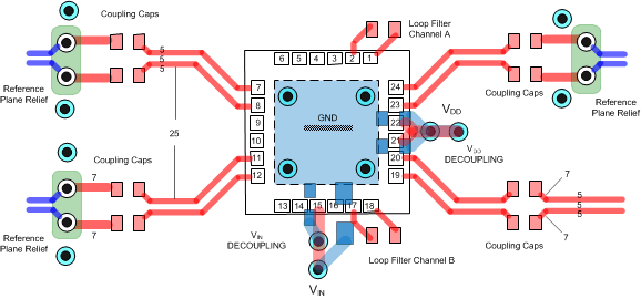
The high speed inputs and outputs have been optimized to work with interconnects using a controlled differential impedance of 100Ω. Vias should be used sparingly and must be placed symmetrically for each side of a given differential pair. Whenever differential vias are used the layout must also provide for a low inductance path for the return currents as well. Route the differential signals away from other signals and noise sources on the printed circuit board.
Figure 13 highlights good high-speed layout techniques.
- Maintain differential pair symmetry to minimize any signal conversion to common mode.
- Isolate Tx - Rx differential pairs with a minimum of 5x inter-pair to intra-pair spacing ratio.
- Decoupling should be placed as close as possible to the DS125DF111
- Use differential vias which incorporate reference plane current returns and relief to minimize impedance disruption.
- Use a back-drill technique to minimize via stubs.
- Keep Loop Filter capacitors as close as possible to the DS125DF111.
10.2 Layout Example
 Figure 13. DS125DF111 Typical Layout