SNLS482B April 2014 – January 2017 DS125DF1610
PRODUCTION DATA.
- 1 Features
- 2 Applications
- 3 Description
- 4 Revision History
- 5 Pin Configuration and Functions
- 6 Specifications
-
7 Detailed Description
- 7.1 Overview
- 7.2 Functional Block Diagram
- 7.3
Feature Description
- 7.3.1 Device Data Path Operation
- 7.3.2 AC-Coupled Receiver with Signal Detect
- 7.3.3 CTLE
- 7.3.4 Cross Point Switch
- 7.3.5 DFE with VGA
- 7.3.6 Clock and Data Recovery
- 7.3.7 Reference Clock
- 7.3.8 Differential Driver with FIR Filter
- 7.3.9 Setting the Output VOD
- 7.3.10 Output Driver Polarity Inversion
- 7.3.11 Driver Output Rise/Fall Time
- 7.3.12 Debug Features
- 7.3.13 Interrupt Signals
- 7.3.14 Other Features
- 7.4 Device Functional Modes
- 7.5 Programming
- 8 Application and Implementation
- 9 Power Supply Recommendations
- 10Layout
- 11Device and Documentation Support
- 12Mechanical, Packaging, and Orderable Information
Package Options
Mechanical Data (Package|Pins)
- ABB|196
Thermal pad, mechanical data (Package|Pins)
Orderable Information
8 Application and Implementation
NOTE
Information in the following applications sections is not part of the TI component specification, and TI does not warrant its accuracy or completeness. TI’s customers are responsible for determining suitability of components for their purposes. Customers should validate and test their design implementation to confirm system functionality.
8.1 Application Information
The DS125DF1610 is a 16 channel retimer that support many different data rates and application spaces. The following sections describe the typical use cases and common implementation practices.
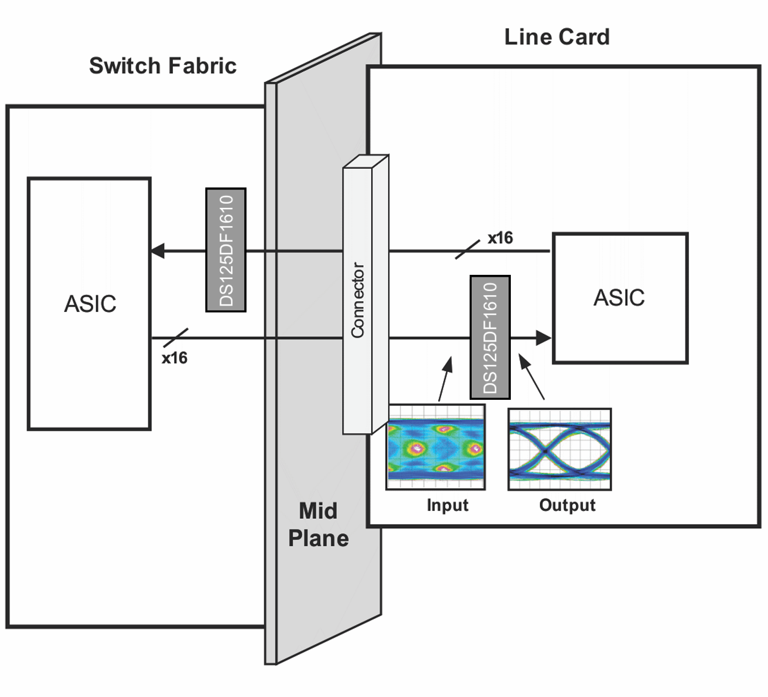 Figure 5. DS125DF1610 Example Application
8.2 Typical Applications
Figure 5 shows a typical implementation for the DS125DF1610 in a back plane application. The DS125DF1610 can also be used for front port applications. The DS125DF1610 supports data rates for CPRI, Infiniband, Ethernet, Interlaken and other custom data rates.
Figure 6 and Figure 7 show a typical application of the DS125DF1610. In these diagrams, the DS125DF1610 is configured for SMBus slave mode programming. Power is supplied to the device through a single 2.5 V plane. The power supply filtering shown in these diagrams may need to be adjusted to accommodate additional system power noise. The SMBus and LVCMOS signals in this example use 2.5 V logic. A differential reference clock for the digital block is applied to the device through 1 µF AC-coupling capacitors. In this example, the high speed signals are connected to the device in groups of four to allow for the system designer to make use of the 4x4 cross point switches. Note that since the device contains AC-coupling capacitors on the high speed receiver inputs, the signals can be directly connected to the device. The transmitter outputs of this device should connect to AC-coupling capacitors placed near the receive inputs of the receiving ASIC.
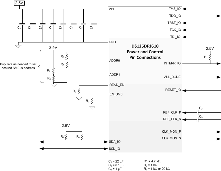 Figure 6. Typical Connection Diagram: Power and Control Pins
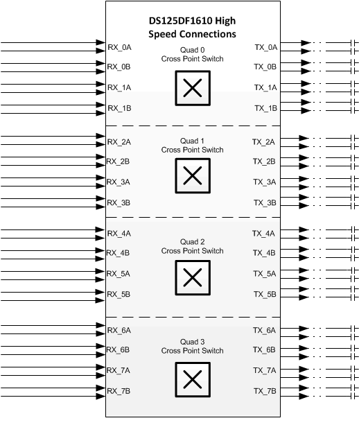 Figure 7. Typical Connection Diagram: High Speed Signals
8.2.1 Design Requirements
This section lists some critical areas for high speed printed circuit board design consideration and study.
- Utilize 100Ω differential impedance traces.
- Back-drill connector vias and signal vias to minimize stub length.
- Use reference plane vias to ensure a low inductance path for the return current.
- Place AC-Coupling capacitors for the transmitter links near the receiver for that channel.
- The maximum body size for AC-coupling capacitors is 0402.
8.2.2 Detailed Design Procedure
To begin the design process determine the following:
- Maximum power draw for PCB regulator selection. For this calculation use the CDR locking power number specified in the datasheet, multiplied by the number of channels allowed to lock at a time by the lock sequencer. Then add the static power. The lock sequencer defaults to 8 channels allowed to lock at a time. To ease the peak power draw, the lock sequencer can be set to allow for only 1 channel to lock at a time. The lock time for each channel is typically very short, so this power calculation should not be used for the thermal simulations of the PCB.
- Maximum operational power for thermal calculations. For this calculation use the CDR locked power numbers specified in the datasheet, multiplied by the number of channels that will be active in the device. Then add the static power. If it is desired to use the Pattern Generator or PRBS checker, add these powers per channel. Note that a channel's PRBS Checker and Pattern Generator cannot both be active at the same time. So the total count of active PRBS Checkers and Pattern Generators should not be more than 16 per device.
- Select a reference clock frequency and routing scheme.
- Plan out channel connectivity. Be sure to note any desired cross point routing in the board schematics.
- Ensure that each device has a unique SMBus address if the control bus is shared with other devices or components.
- Use the IBIS-AMI model for simple channel simulations before PCB layout is complete.
- Compare schematic against the typical connection diagrams in the datasheet, Figure 6 and Figure 7
8.2.3 Typical Application Performance Plots
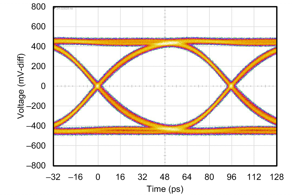 Figure 8. Typical Transmit Eye Diagram, 10.3125 Gbps
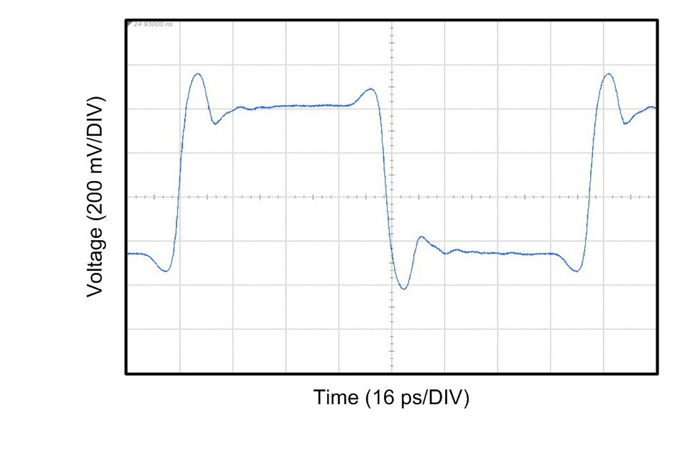 Figure 9. FIR Transmit Equalization Example, 10.3125Gbps
Figure 8 shows a typical output eye diagram for the DS125DF1610 operating at 10.3125 Gbps with the 1VPP VOD settings. All other device settings are left at default.
Figure 9 shows an example of FIR transmit equalization for a DS125DF1610 operating at 10.3125 Gbps. In this example, the high speed output is configured for 1VPP VOD. The FIR filter is then further adjusted such that the pre cursor tap is set to -5, the main cursor tap is set to +42, and the post cursor tap is set to -10. An 8T pattern is used to evaluate the FIR filter, which consists of 0xFF00. All other device settings are left at default.
8.3 Initialization Setup
The typical device initialization sequence for a DS125DF1610 includes the following:
- Shared Register Configurations:
- Reference Clock Divider Setting (default is 25MHz)
- Lock Sequencer Configuration (default is 8 channels allowed lock concurrently)
- Channel Register Configurations repeated for all desired channels:
- CDR reset
- Adapt Mode Configuration
- Data rate selection
- Output driver VOD and FIR configuration
- Optional Continuous DFE adaption configuration
- Optional Interrupt enable
- Optional Reference clock loop through enable
- Optional Cross point switch configuration
- CDR reset release
8.3.1 Data Rate Selection (Rate/Sub-Rate Table)
The data rates for the DS125DF1610 must be known and programmed into each desired channel. The DS125DF1610 will only lock to programmed data rates and the programmed divider settings. For ease of use several common data rates have been preprogrammed into the DS125DF1610 along with the associated sub-rates for those various standards. These rate/sub-rate settings comprise the Rate/Sub-rate Table 18. Note that each channel operates independently, so different channels in the DS125DF1610 can operate at different data rates at the same time.
The Rate/Sub-rate Table 18 for the DS125DF1610 shown below includes all of the available preprogrammed data rates and associated divider groupings.
Table 18. Rate/Sub-Rate Options
| CHANNEL REGISTER 0x2F[7:4] SETTING | STANDARD | DATA RATES (Gbps) | FIRST GROUP DIVIDER SETTINGS | SECOND GROUP DIVIDER SETTINGS |
|---|---|---|---|---|
| 0x6 | Custom | 11.5 | 1 | 1 |
| 0x7 | Interlaken | 12.5, 6.25, 3.125 | 1, 2, 4 | 1, 2, 4 |
| 0x8 | CPRI 1 | 9.8304, 4.9152, 2.4576 | 1, 2, 4 | 1, 2, 4 |
| 0x9 | CPRI 2 | 6.144, 3.072 | 2, 4 | 2, 4 |
| 0xA | Infiniband | 10, 5, 2.5 | 1, 2, 4 | 1, 2, 4 |
| 0xB | Ethernet | 10.3125, 1.25 | 8 | 1 |
8.3.2 Data Rate Selection (Manual Programming)
The DS125DF1610 is capable of supporting any data rate within the specified range of 9.8 Gbps to 12.5 Gbps including the divide by 2, 4, and 8 sub-rates of this range. If it is desired to operate the DS125DF1610 at a data rate or data rate and sub-rate combination that is not available in the Rate/Sub-rate Table 18, then these desired data rates can be programmed into the device manually.
The following procedure describes how to calculate and manually program data rates into the DS125DF1610.
- Select a divider grouping from the Rate/Sub-rate Table and program that value to channel register 0x2F. When manually programming the data rate into the device, other rate/sub-rate values may be used to allow for different divider and group combinations. A list of all preprogrammed divider, group combinations is shown in the Table 19 below.
- Calculate the first group settings:
- Calculate the second group settings:
Table 19. Divider Options
| CHANNEL REGISTER 0x2F[7:4] SETTING |
FIRST GROUP DIVIDER SETTINGS | SECOND GROUP DIVIDER SETTINGS |
|---|---|---|
| 0x0 | 2, 4 | 2, 4 |
| 0x1 | 1 | 1 |
| 0x2 | 1, 2, 4 | 1, 2, 4 |
| 0x3 | 1, 2, 4 | 1, 2, 4 |
| 0x4 | 1 | 1 |
| 0x5 | 1 | 1 |
| 0x6 | 1 | 1 |
| 0x7 | 1, 2, 4 | 1, 2, 4 |
| 0x8 | 1, 2, 4 | 1, 2, 4 |
| 0x9 | 2, 4 | 2, 4 |
| 0xA | 1, 2, 4 | 1, 2, 4 |
| 0xB | 8 | 1 |
| 0xC | 8 | 1 |
| 0xD | 1, 2, 4 | 1 |
| 0xE | 1 | 1 |
| 0xF | 1, 2 | 1, 2 |
Table 20. Manual Data Rate Configuration -- 1STGroup Instructions
| PARAMETER | VALUE/EQUATION | COMMENT |
|---|---|---|
| Reference Clock | F0 = 25e6 | Internally the reference clock always operates at 25 MHz |
| Desired VCO Frequency | F1 | F1 is the frequency of the VC0 which is equal to the desired data rate. If the desired data rate uses dividers, be sure to multiply the data rate by the divide setting to get the correct VCO frequency |
| Number of Reference Clocks | N = 1024 | |
| VCO Freq ÷ 32 | F2 = F1 ÷ 32 | |
| Counts of VCO Freq ÷ 32 required | F3 = F2 x N ÷ F0 | |
| Counts of VCO Freq ÷ 32 required rounded | F4 | Round F3 to the nearest integer value. Convert this value to binary. Program the upper 8 bits to ch register 0x61 and the lower 8 bits to ch register 0x60. Be sure to set channel register 0x61[7] to 1 to enable the override function for manual programming. |
| PPM error due to rounding | Err = 1e6 x (F4 – F3) ÷ F3 | |
| Required PPM tolerance | T | Enter the desired PPM tolerance |
| VCO Freq ÷ 32 +PPM tolerance | F5 = (1+ T÷1e6) * F2 | |
| Rounded Counts of the VCO Freq ÷ 32 +PPM tolerance required | F6 = F5 x N ÷ F0 | Round F6 to the nearest integer value |
| PPM Counts delta | F7 = F6 – F3 | Convert this value to binary. Program the most significant bit channel register 0x67[7] and the rest of the bits to channel register 0x64[7:4] |
Table 21. Manual Data Rate Configuration -- 2ndGroup Instructions
| PARAMETER | VALUE/EQUATION | COMMENT |
|---|---|---|
| Reference Clock | F0 = 25e6 | Internally the reference clock always operates at 25 MHz |
| Desired VCO Frequency | F1 | F1 is the frequency of the VC0 which is equal to the desired data rate. If the desired data rate uses dividers, be sure to multiply the data rate by the divide setting to get the correct VCO frequency |
| Number of Reference Clocks | N = 1024 | |
| VCO Freq ÷ 32 | F2 = F1 ÷ 32 | |
| Counts of VCO Freq ÷ 32 required | F3 = F2 x N ÷ F0 | |
| Counts of VCO Freq ÷ 32 required rounded | F4 | Round F3 to the nearest integer value. Convert this value to binary. Program the upper 8 bits to ch register 0x63 and the lower 8 bits to ch register 0x62. Be sure to set channel register 0x63[7] to 1 to enable the override function for manual programming. |
| PPM error due to rounding | Err = 1e6 x (F4 – F3) ÷ F3 | |
| Required PPM tolerance | T | Enter the desired PPM tolerance |
| VCO Freq ÷ 32 +PPM tolerance | F5 = (1+ T÷1e6) * F2 | |
| Rounded Counts of the VCO Freq ÷ 32 +PPM tolerance required | F6 = F5 x N ÷ F0 | Round F6 to the nearest integer value |
| PPM Counts delta | F7 = F6 – F3 | Convert this value to binary. Program the most significant bit channel register 0x67[6] and the rest of the bits to channel register 0x64[3:0] |
An example for setting group 0 and group 1 to 11.3 Gbps is shown in the Table 22 below.
Table 22. Manual Data Rate Configuration Example
| CHANNEL REGISTER (HEX) | VALUE |
|---|---|
| 0x60 | 0x80 |
| 0x61 | 0xB8 |
| 0x62 | 0x80 |
| 0x63 | 0xB8 |
| 0x64 | 0xEE |
| 0x67[7:6] | 2'b00 |