SNLS685 December 2020 DS160PR412
PRODUCTION DATA
- 1 Features
- 2 Applications
- 3 Description
- 4 Revision History
- 5 Pin Configuration and Functions
- 6 Specifications
- 7 Detailed Description
- 8 Application and Implementation
- 9 Power Supply Recommendations
- 10Layout
- 11Layout Example
- 12Device and Documentation Support
- 13Mechanical, Packaging, and Orderable Information
Package Options
Mechanical Data (Package|Pins)
- RUA|42
Thermal pad, mechanical data (Package|Pins)
- RUA|42
Orderable Information
11 Layout Example
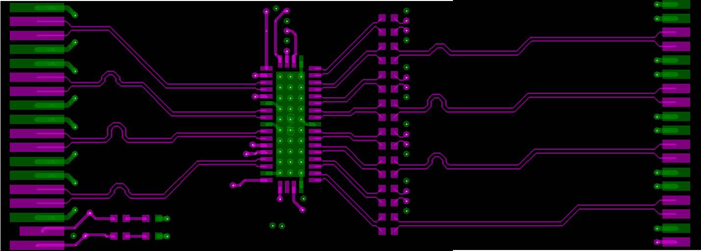
Figure 11-1 shows DS160PR412 layout example.
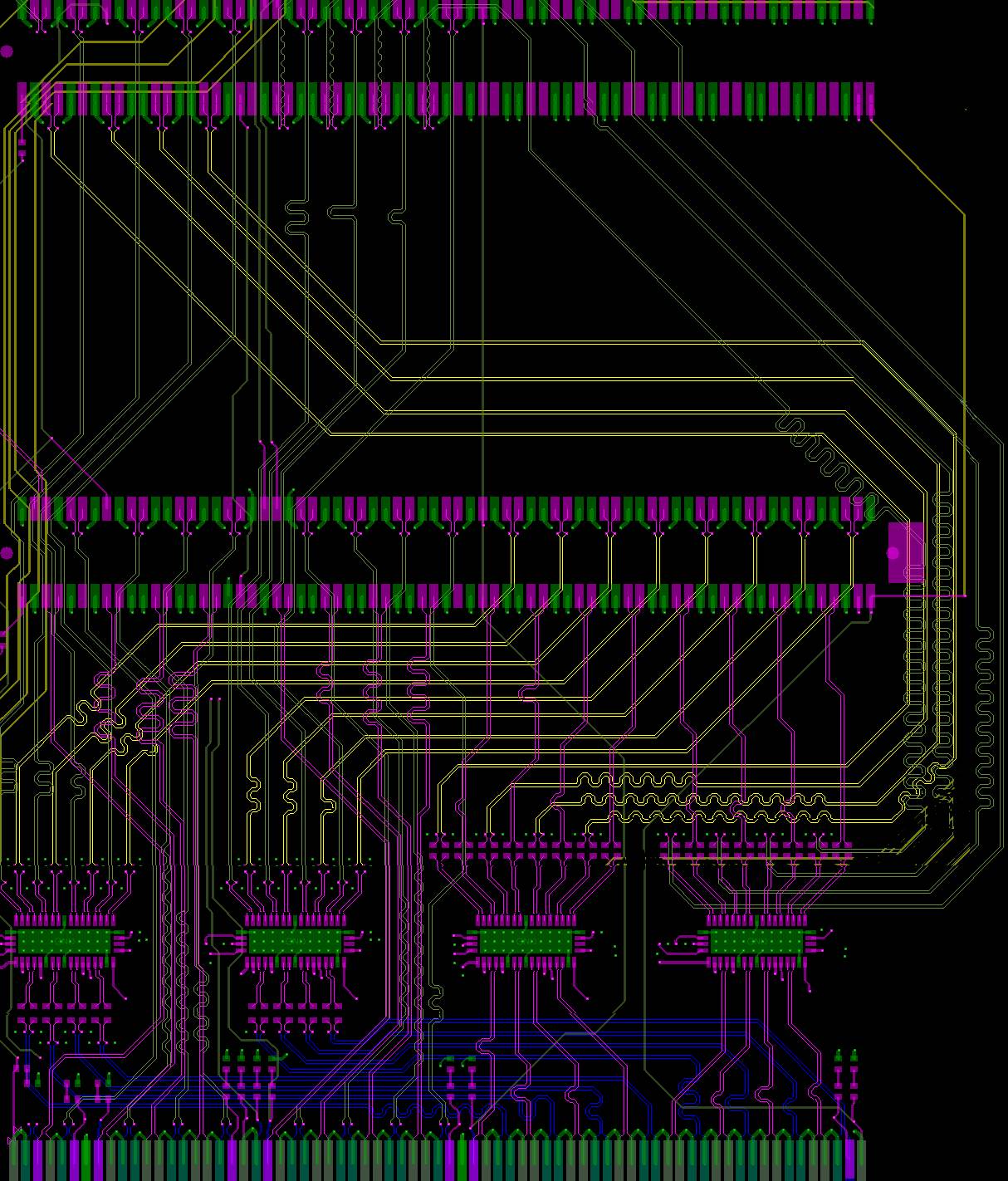
 Figure 11-1 DS160PR412 layout exampleFigure 11-2 shows a layout illustration
where two DS160PR412 and two DS160PR421 are used to switch 8 lanes between two PCIe slots.
 Figure 11-2 Layout example for PCIe lane muxing
application
 Figure 11-1 DS160PR412 layout example
 Figure 11-2 Layout example for PCIe lane muxing
application