SNLS689 December   2020 DS160PR822

PRODUCTION DATA  

  1. Features
  2. Applications
  3. Description
  4. Revision History
  5. Pin Configuration and Functions
    1.     Pin Functions
  6. Specifications
    1. 6.1 Absolute Maximum Ratings
    2. 6.2 ESD Ratings
    3. 6.3 Recommended Operating Conditions
    4. 6.4 Thermal Information
    5. 6.5 DC Electrical Characteristics
    6. 6.6 High Speed Electrical Characteristics
    7. 6.7 SMBUS/I2C Timing Characteristics
    8. 6.8 Typical Characteristics
  7. Detailed Description
    1. 7.1 Overview
    2. 7.2 Functional Block Diagram
    3. 7.3 Feature Description
      1. 7.3.1 Linear Equalization
      2. 7.3.2 Flat Gain
      3. 7.3.3 Receiver Detect State Machine
      4. 7.3.4 Cross Point
    4. 7.4 Device Functional Modes
      1. 7.4.1 Active PCIe Mode
      2. 7.4.2 Active Buffer Mode
      3. 7.4.3 Standby Mode
    5. 7.5 Programming
      1. 7.5.1 Control and Configuration Interface
        1. 7.5.1.1 Pin Mode
          1. 7.5.1.1.1 Four-Level Control Inputs
        2. 7.5.1.2 SMBUS/I2C Register Control Interface
        3. 7.5.1.3 SMBus/I 2 C Master Mode Configuration (EEPROM Self Load)
  8. Application and Implementation
    1. 8.1 Application Information
    2. 8.2 Typical Applications
      1. 8.2.1 37
        1. 8.2.1.1 Design Requirements
        2. 8.2.1.2 Detailed Design Procedure
        3. 8.2.1.3 Application Curves
  9. Power Supply Recommendations
  10. 10Layout
    1. 10.1 Layout Guidelines
    2. 10.2 Layout Example
  11. 11Device and Documentation Support
    1. 11.1 Receiving Notification of Documentation Updates
    2. 11.2 Community Resources
    3. 11.3 Trademarks
  12. 12Mechanical, Packaging, and Orderable Information

Package Options

Mechanical Data (Package|Pins)
Thermal pad, mechanical data (Package|Pins)
Orderable Information

Typical Characteristics

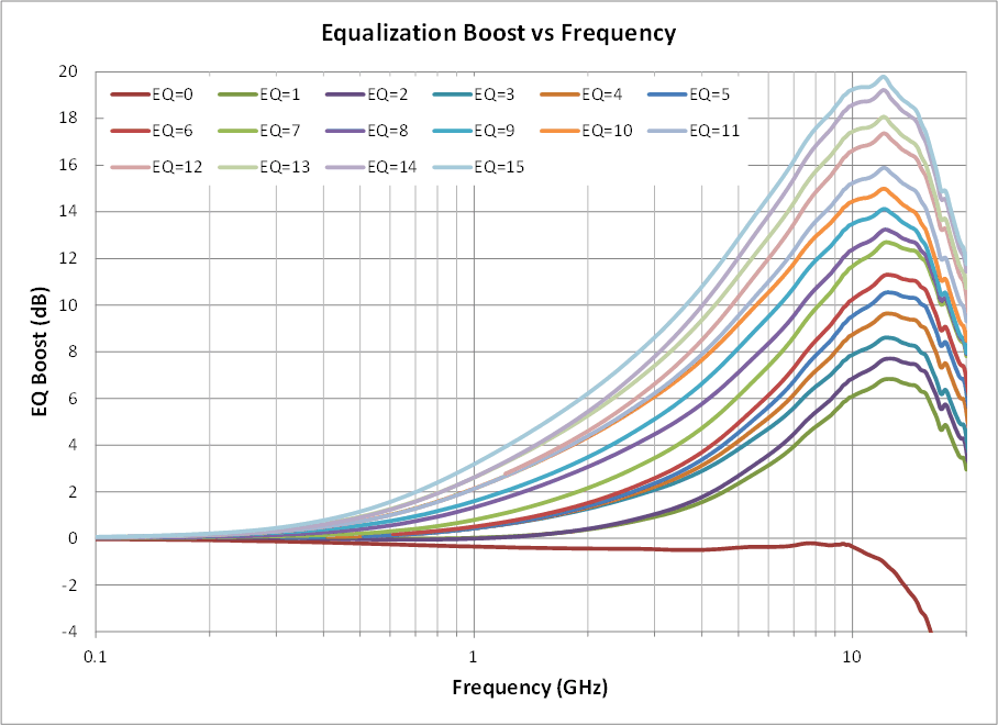
GUID-20201018-CA0I-6RLD-XXLK-LSVN3DKRX39Q-low.gif Figure 6-1 Typical EQ Boost vs Frequency
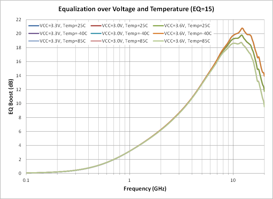
GUID-20201018-CA0I-JNDX-D1KX-KHKXZSB9XFCN-low.gif Figure 6-2 Typical EQ Boost over Voltage and Temperature with EQ=15
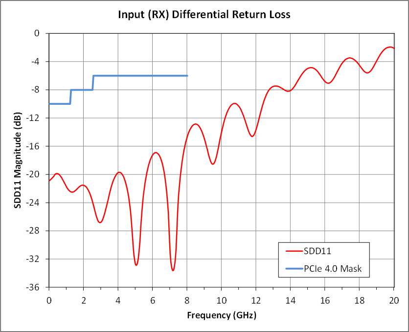
GUID-20201018-CA0I-MVLR-PZ4R-VQXSMDTPCCS1-low.gif Figure 6-3 Typical RX Differential Return Loss
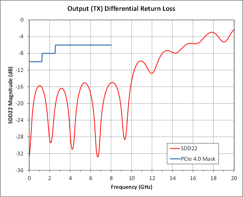
GUID-20201018-CA0I-CQ1N-2PHV-1C5THFLZPTN8-low.gif Figure 6-4 Typical TX Differential Return Loss
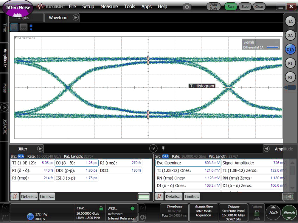
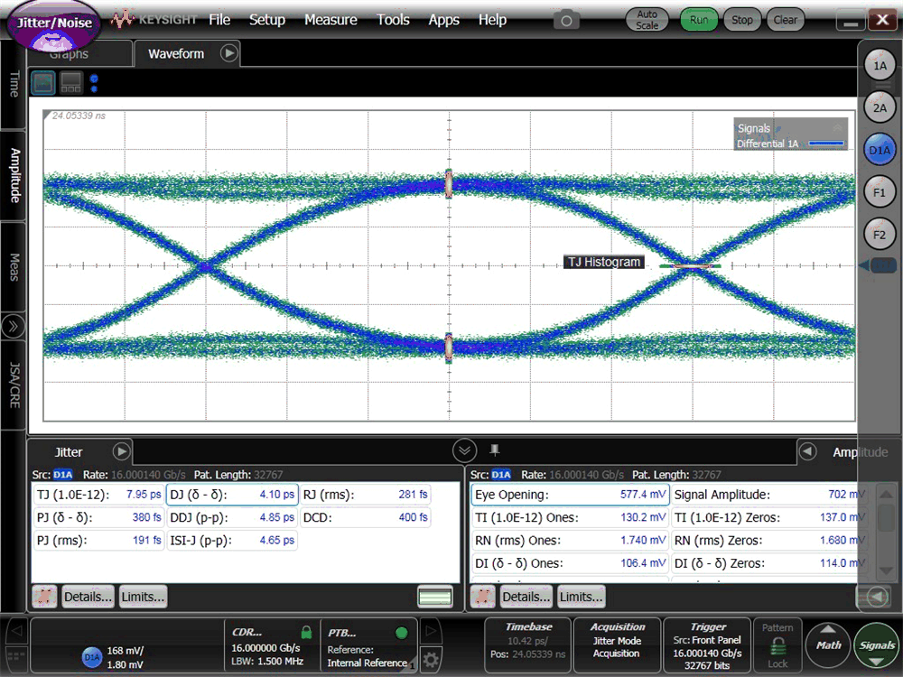
GUID-20201111-CA0I-KRKT-D4NJ-QMJJNM6TFP1L-low.gif GUID-20201111-CA0I-BCW5-ZPVT-MCP8CDTWKLSV-low.gif Figure 6-5 Typical Jitter Characteristics - Top: 16Gbps PRBS15 Input to the Device, Bottom: Output of the Device.