SNLS045C July 1999 – July 2016 DS90LV048A
PRODUCTION DATA.
- 1 Features
- 2 Applications
- 3 Description
- 4 Revision History
- 5 Pin Configuration and Functions
- 6 Specifications
- 7 Parameter Measurement Information
- 8 Detailed Description
- 9 Application and Implementation
- 10Power Supply Recommendations
- 11Layout
- 12Device and Documentation Support
- 13Mechanical, Packaging, and Orderable Information
Package Options
Mechanical Data (Package|Pins)
Thermal pad, mechanical data (Package|Pins)
Orderable Information
9 Application and Implementation
NOTE
Information in the following applications sections is not part of the TI component specification, and TI does not warrant its accuracy or completeness. TI’s customers are responsible for determining suitability of components for their purposes. Customers should validate and test their design implementation to confirm system functionality.
9.1 Application Information
The DS90LV048A has a flow-through pinout that allows for easy PCB layout. The LVDS signals on one side of the device easily allows for matching electrical lengths of the differential pair trace lines between the driver and the receiver as well as allowing the trace lines to be close together to couple noise as common-mode. Noise isolation is achieved with the LVDS signals on one side of the device and the TTL signals on the other side.
9.2 Typical Application
 Figure 19. Balanced System Point-to-Point Application
9.2.1 Design Requirements
When using LVDS devices, it is important to remember to specify controlled impedance PCB traces, cable assemblies, and connectors. All components of the transmission media must have a matched differential impedance of about 100 Ω. They must not introduce major impedance discontinuities.
Balanced cables (for example, twisted pair) are usually better than unbalanced cables (ribbon cable) for noise reduction and signal quality. Balanced cables tend to generate less EMI due to field canceling effects and also tend to pick up electromagnetic radiation as common-mode (not differential mode) noise which is rejected by the LVDS receiver.
For cable distances < 0.5 M, most cables can be made to work effectively. For distances 0.5 M ≤ d ≤ 10 M, CAT5 (Category 5) twisted pair cable works well, is readily available, and relatively inexpensive.
9.2.2 Detailed Design Procedure
9.2.2.1 Probing LVDS Transmission Lines
Always use high impedance (> 100kΩ), low capacitance (< 2 pF) scope probes with a wide bandwidth (1 GHz) scope. Improper probing gives deceiving results.
9.2.2.2 Threshold
The LVDS Standard (ANSI/TIA/EIA-644) specifies a maximum threshold of ±100 mV for the LVDS receiver. The DS90LV048A supports an enhanced threshold region of −100 mV to 0 V. This is useful for fail-safe biasing. The threshold region is shown in the Voltage Transfer Curve (VTC) in Figure 20. The typical DS90LV048A LVDS receiver switches at about −35 mV.
NOTE
With VID = 0 V, the output is in a HIGH state. With an external fail-safe bias of +25 mV applied, the typical differential noise margin is now the difference from the switch point to the bias point.
In the following example, this would be 60 mV of Differential Noise Margin (+25 mV − (−35 mV)). With the enhanced threshold region of −100 mV to 0 V, this small external fail-safe biasing of +25 mV (with respect to
0 V) gives a DNM of a comfortable 60 mV. With the standard threshold region of ±100 mV, the external fail-safe biasing would need to be +25 mV with respect to +100 mV or +125 mV, giving a DNM of 160 mV which is stronger fail-safe biasing than is necessary for the DS90LV048A. If more DNM is required, then a stronger fail-safe bias point can be set by changing resistor values.
 Figure 20. VTC of the DS90LV048A LVDS Receiver
9.2.3 Application Curve
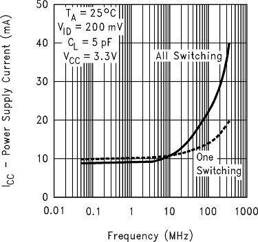
 Figure 21. Power Supply Current vs Frequency