SNLS433C November 2012 – January 2015 DS90UH927Q-Q1
PRODUCTION DATA.
- 1 Features
- 2 Applications
- 3 Description
- 4 Revision History
- 5 Pin Configuration and Functions
-
6 Specifications
- 6.1 Absolute Maximum Ratings
- 6.2 ESD Ratings
- 6.3 Recommended Operating Conditions
- 6.4 Thermal Information
- 6.5 DC Electrical Characteristics
- 6.6 AC Electrical Characteristics
- 6.7 DC and AC Serial Control Bus Characteristics
- 6.8 Recommended Timing Requirements for the Serial Control Bus
- 6.9 Timing Requirements
- 6.10 Typical Characteristics
-
7 Detailed Description
- 7.1 Overview
- 7.2 Functional Block Diagram
- 7.3
Feature Description
- 7.3.1 High-Speed Forward Channel Data Transfer
- 7.3.2 Low-Speed Back Channel Data Transfer
- 7.3.3 Common Mode Filter Pin (CMF)
- 7.3.4 Video Control Signals
- 7.3.5 EMI Reduction Features
- 7.3.6 Built-In Self Test (BIST)
- 7.3.7 Forward Channel and Back Channel Error Checking
- 7.3.8 Internal Pattern Generation
- 7.3.9 Remote Auto Power Down Mode
- 7.3.10 Input RxCLKIN Loss Detect
- 7.3.11 Serial Link Fault Detect
- 7.3.12 INTERRUPT Pin (INTB)
- 7.3.13 General-Purpose I/O
- 7.3.14 I2S Audio Interface
- 7.3.15 Additional Features
- 7.4 Device Functional Modes
- 7.5 Programming
- 7.6 Register Maps
- 8 Application and Implementation
- 9 Power Supply Recommendations
- 10Layout
- 11Device and Documentation Support
- 12Mechanical, Packaging, and Orderable Information
Package Options
Mechanical Data (Package|Pins)
- RTA|40
Thermal pad, mechanical data (Package|Pins)
- RTA|40
Orderable Information
1 Features
- Integrated HDCP Cipher Engine with On-Chip Key Storage
- Bidirectional Control Channel Interface with I2C Compatible Serial Control Bus
- Low EMI FPD-Link Video Input
- Supports High Definition (720p) Digital Video Format
- 5-MHz to 85-MHz PCLK Supported
- RGB888 + VS, HS, DE and I2S Audio Supported
- Up to 4 I2S Digital Audio Inputs for Surround Sound Applications
- 4 Bidirectional GPIO Channels with 2 Dedicated Pins
- Single 3.3-V Supply with 1.8-V or 3.3-V Compatible LVCMOS I/O Interface
- AC-Coupled STP Interconnect up to 10 Meters
- DC-Balanced & Scrambled Data with Embedded Clock
- Supports HDCP Repeater Application
- Internal Pattern Generation
- Low Power Modes Minimize Power Dissipation
- Automotive Grade Product: AEC-Q100 Grade 2 Qualified
- > 8-kV HBM and ISO 10605 ESD Rating
- Backward Compatible Modes
2 Applications
- Automotive Displays for Navigation
- Rear Seat Entertainment Systems
3 Description
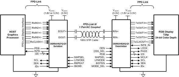
The DS90UH927Q-Q1 serializer, in conjunction with a DS90UH928Q-Q1 or DS90UH926Q-Q1 deserializer, provides a solution for secure distribution of content-protected digital video within automotive entertainment systems. This chipset translates a FPD-Link video interface into a single-pair high-speed serialized interface. The digital video data is protected using the industry standard High-Bandwidth Digital Content Protection (HDCP) copy protection scheme. The FPD-Link III serial bus scheme supports full duplex, high speed forward channel data transmission and low-speed back channel communication over a single differential link. Consolidation of audio, video, and control data over a single differential pair reduces the interconnect size and weight, while also eliminating skew issues and simplifying system design.
The DS90UH927Q-Q1 serializer embeds the clock, content protects the data payload, and level shifts the signals to high-speed differential signaling. Up to 24 RGB data bits are serialized along with three video control signals, and up to four I2S data inputs.
The FPD-Link data interface allows for easy interfacing with data sources while also minimizing EMI and bus width. EMI on the high-speed FPD-Link III bus is minimized using low voltage differential signaling, data scrambling and randomization, and dc-balancing.
The HDCP cipher engine is implemented in both the serializer and deserializer. HDCP keys are stored in on-chip memory.
Device Information(1)
| PART NUMBER | PACKAGE | BODY SIZE (NOM) |
|---|---|---|
| DS90UH927Q-Q1 | WQFN (40) | 6.00 mm x 6.00 mm |
- For all available packages, see the orderable addendum at the end of the data sheet.
Application Diagram