SNLS433C November 2012 – January 2015 DS90UH927Q-Q1
PRODUCTION DATA.
- 1 Features
- 2 Applications
- 3 Description
- 4 Revision History
- 5 Pin Configuration and Functions
-
6 Specifications
- 6.1 Absolute Maximum Ratings
- 6.2 ESD Ratings
- 6.3 Recommended Operating Conditions
- 6.4 Thermal Information
- 6.5 DC Electrical Characteristics
- 6.6 AC Electrical Characteristics
- 6.7 DC and AC Serial Control Bus Characteristics
- 6.8 Recommended Timing Requirements for the Serial Control Bus
- 6.9 Timing Requirements
- 6.10 Typical Characteristics
-
7 Detailed Description
- 7.1 Overview
- 7.2 Functional Block Diagram
- 7.3
Feature Description
- 7.3.1 High-Speed Forward Channel Data Transfer
- 7.3.2 Low-Speed Back Channel Data Transfer
- 7.3.3 Common Mode Filter Pin (CMF)
- 7.3.4 Video Control Signals
- 7.3.5 EMI Reduction Features
- 7.3.6 Built-In Self Test (BIST)
- 7.3.7 Forward Channel and Back Channel Error Checking
- 7.3.8 Internal Pattern Generation
- 7.3.9 Remote Auto Power Down Mode
- 7.3.10 Input RxCLKIN Loss Detect
- 7.3.11 Serial Link Fault Detect
- 7.3.12 INTERRUPT Pin (INTB)
- 7.3.13 General-Purpose I/O
- 7.3.14 I2S Audio Interface
- 7.3.15 Additional Features
- 7.4 Device Functional Modes
- 7.5 Programming
- 7.6 Register Maps
- 8 Application and Implementation
- 9 Power Supply Recommendations
- 10Layout
- 11Device and Documentation Support
- 12Mechanical, Packaging, and Orderable Information
Package Options
Mechanical Data (Package|Pins)
- RTA|40
Thermal pad, mechanical data (Package|Pins)
- RTA|40
Orderable Information
6 Specifications
6.1 Absolute Maximum Ratings(1)(2)(3)
| MIN | MAX | UNIT | |
|---|---|---|---|
| Supply Voltage – VDD33(4) | −0.3 | 4.0 | V |
| Supply Voltage – VDDIO(4) | −0.3 | 4.0 | V |
| LVCMOS I/O Voltage | −0.3 | (VDDIO + 0.3) | V |
| Serializer Output Voltage | −0.3 | 2.75 | V |
| Junction Temperature | 150 | °C | |
| Storage Temperature, Tstg | −65 | 150 | °C |
(1) Stresses beyond those listed under Absolute Maximum Ratings may cause permanent damage to the device. These are stress ratings only, which do not imply functional operation of the device at these or any other conditions beyond those indicated under Recommended Operating Conditions. Exposure to absolute-maximum-rated conditions for extended periods may affect device reliability.
(2) For soldering specifications, see product folder at www.ti.com and www.ti.com/lit/an/snoa549c/snoa549c.pdf.
(3) If Military/Aerospace specified devices are required, please contact the Texas Instruments Sales Office/Distributors for availability and specifications.
(4) The DS90UH927Q-Q1 VDD33 and VDDIO voltages require a specific ramp rate during power up. The power supply ramp time must be less than 1.5 ms with a monotonic rise
6.2 ESD Ratings
| VALUE | UNIT | |||||
|---|---|---|---|---|---|---|
| V(ESD) | Electrostatic discharge | Human body model (HBM), per AEC Q100-002(1) | ±8000 | V | ||
| Charged device model (CDM), per AEC Q100-011 | ±1250 | |||||
| Machine model (MM) | ±250 | |||||
| (IEC 61000-4-2, powered-up only) RD = 330 Ω, CS = 150 pF |
Air Discharge (Pin 16 and 17) |
±15000 | V | |||
| Contact Discharge (Pin 16 and 17) |
±8000 | |||||
| (ISO 10605) RD = 330 Ω, CS = 150 pF/330 pF RD = 2 kΩ, CS = 150 pF/330 pF |
Air Discharge (Pin 16 and 17) |
±15000 | ||||
| Contact Discharge (Pin 16 and 17) |
±8000 | |||||
(1) AEC Q100-002 indicates HBM stressing is done in accordance with the ANSI/ESDA/JEDEC JS-001 specification.
6.3 Recommended Operating Conditions
| MIN | NOM | MAX | UNIT | ||
|---|---|---|---|---|---|
| Supply Voltage (VDD33) | 3 | 3.3 | 3.6 | V | |
| LVCMOS Supply Voltage (VDDIO)(2) | Connect VDDIO to 3.3 V and use 3.3-V IOs | 3 | 3.3 | 3.6 | V |
| Connect VDDIO to 1.8 V and use 1.8-V IOs | 1.71 | 1.8 | 1.89 | V | |
| Operating Free Air Temperature (TA) | −40 | +25 | +105 | °C | |
| PCLK Frequency | 5 | 85 | MHz | ||
| Supply Noise(1) | 100 | mVP-P | |||
(1) Supply noise testing was done with minimum capacitors on the PCB. A sinusoidal signal is AC coupled to the VDD33 and VDDIOsupplies with amplitude = 100 mVp-p measured at the device VDD33 and VDDIO pins. Bit error rate testing of input to the Ser and output of the Des with 10 meter cable shows no error when the noise frequency on the Ser is less than 50 MHz. The Des on the other hand shows no error when the noise frequency is less than 50 MHz.
(2) VDDIO < VDD33 + 0.3 V
6.4 Thermal Information
| THERMAL METRIC(1) | DS90UH927Q-Q1 | UNIT | |
|---|---|---|---|
| RTA (WQFN) | |||
| 40 PINS | |||
| RθJA | Junction-to-ambient thermal resistance | 29.0 | °C/W |
| RθJC(top) | Junction-to-case (top) thermal resistance | 14.4 | |
| RθJB | Junction-to-board thermal resistance | 5.1 | |
| ψJT | Junction-to-top characterization parameter | 0.2 | |
| ψJB | Junction-to-board characterization parameter | 5.1 | |
| RθJC(bot) | Junction-to-case (bottom) thermal resistance | 1.4 | |
(1) For more information about traditional and new thermal metrics, see the IC Package Thermal Metrics application report, SPRA953.
6.5 DC Electrical Characteristics
Over recommended operating supply and temperature ranges unless otherwise specified.(1)(2)(3)| PARAMETER | TEST CONDITIONS | PIN/FREQ. | MIN | TYP | MAX | UNIT | ||
|---|---|---|---|---|---|---|---|---|
| LVCMOS I/O | ||||||||
| VIH | High Level Input Voltage | VDDIO = 3.0 V to 3.6 V(4) | PDB | 2.0 | VDDIO | V | ||
| VIL | Low Level Input Voltage | VDDIO = 3.0 V to 3.6 V(4) | GND | 0.8 | V | |||
| IIN | Input Current | VIN = 0 V or VDDIO = 3.0 V to 3.6 V(4) | −15 | ±1 | +15 | μA | ||
| VIH | High Level Input Voltage | VDDIO = 3.0 V to 3.6 V | GPIO[1:0] I2S_CLK I2S_WC I2S_D [A,B,C,D] LFMODE MAPSEL BKWD REPEAT |
2.0 | VDDIO | V | ||
| VDDIO = 1.71 V to 1.89 V | 0.65× VDDIO |
VDDIO | V | |||||
| VIL | Low Level Input Voltage | VDDIO = 3.0 V to 3.6 V | GND | 0.8 | V | |||
| VDDIO = 1.71 V to 1.89 V | GND | 0.35* VDDIO |
V | |||||
| IIN | Input Current | VIN = 0 V or VDDIO | VDDIO = 3.0 V to 3.6 V | −15 | ±1 | +15 | μA | |
| VDDIO = 1.71 V to 1.89 V | −15 | ±1 | +15 | μA | ||||
| VOH | High Level Output Voltage | IOH = −4 mA | VDDIO = 3.0 V to 3.6 V | GPIO[3:0], GPO_REG [8:5] |
2.4 | VDDIO | V | |
| VDDIO = 1.71 V to 1.89 V | VDDIO - 0.45 | VDDIO | V | |||||
| VOL | Low Level Output Voltage | IOL = +4 mA | VDDIO = 3.0 V to 3.6 V | GND | 0.4 | V | ||
| VDDIO = 1.71 V to 1.89 V | GND | 0.45 | V | |||||
| IOS | Output Short Circuit Current(5) | VOUT = 0 V | −55 | mA | ||||
| IOZ | TRI-STATE® Output Current | VOUT = 0 V or VDDIO, PDB = L, | −15 | +15 | μA | |||
| FPD-LINK LVDS RECEIVER | ||||||||
| VTH | Threshold High Voltage | VCM = 1.2 V | RxCLKIN± RxIN[3:0]± |
+100 | mV | |||
| VTL | Threshold Low Voltage | −100 | mV | |||||
| |VID| | Differential Input Voltage Swing | 200 | 600 | mV | ||||
| VCM | Common Mode Voltage | 0 | 1.2 | 2.4 | V | |||
| IIN | Input Current | −10 | +10 | μA | ||||
| FPD-LINK III CML DRIVER | ||||||||
| VODp-p | Differential Output Voltage (DOUT+) – (DOUT-) |
RL = 100 Ω | DOUT± | 800 | 1000 | 1200 | mVp-p | |
| ΔVOD | Output Voltage Unbalance | 1 | 50 | mV | ||||
| VOS | Offset Voltage – Single-ended | RL = 100 Ω | 2.5-0.25* VODp-p (TYP) |
V | ||||
| ΔVOS | Offset Voltage Unbalance Single-ended |
1 | 50 | mV | ||||
| IOS | Output Short Circuit Current | DOUT+/- = 0V, PDB = L or H | mA | |||||
| RT | Internal Termination Resistance - Differential | 80 | 100 | 120 | Ω | |||
| SUPPLY CURRENT | ||||||||
| IDD1 | Supply Current RL = 100Ω, PCLK = 85MHz |
Checkerboard Pattern | VDD33= 3.6 V | 135 | 160 | mA | ||
| IDDIO1 | VDDIO = 3.6 V | 100 | 500 | μA | ||||
| VDDIO = 1.89 V | 200 | 600 | μA | |||||
| IDD2 | Random Pattern PRBS7 |
VDD33= 3.6 V | 133 | mA | ||||
| IDDIO2 | VDDIO = 3.6 V | 100 | μA | |||||
| VDDIO = 1.89 V | 100 | μA | ||||||
| IDDS | Supply Current — Remote Auto Power Down | reg_0x01[7]=1, Back channel Idle | VDD33 = 3.6 V | 1.2 | 2.4 | mA | ||
| IDDIOS | VDDIO = 3.6 V | 4 | 30 | μA | ||||
| VDDIO = 1.89 V | 5 | 30 | μA | |||||
| IDDZ | Supply Current — Power Down | PDB = 0 V, All other LVCMOS inputs = 0 V | VDD33 = 3.6 V | 1 | 2.2 | mA | ||
| IDDIOZ | VDDIO = 3.6 V | 8 | 20 | μA | ||||
| VDDIO = 1.89 V | 4 | 20 | μA | |||||
(1) The Electrical Characteristics tables list ensured specifications under the listed Recommended Operating Conditions except as otherwise modified or specified by the Electrical Characteristics conditions and/or notes. Typical specifications are estimations only and are not ensured.
(2) Typical values represent most likely parametric norms at VDD33 = 3.3V, VDDIO = 1.8V or 3.3V, TA = 25°C, and at the Recommended Operating Conditions at the time of product characterization and are not ensured.
(3) Current into device pins is defined as positive. Current out of a device pin is defined as negative. Voltages are referenced to ground except VOD and ΔVOD, which are differential voltages. Supply noise testing was done with minimum capacitors on the PCB. A sinusoidal signal is AC coupled to the supply pins with amplitude = 100 mVp-p measured at the device VDD33 and VDDIO pins. Bit error rate testing of input to the serializer and output of the deserializer with 10 meter cable shows no error when the noise frequency is less than 50 MHz.
(4) PDB is specified to 3.3-V LVCMOS only and must be driven or pulled up to VDD33 or to VDDIO ≥ 3.0 V
(5) IOS is not specified for an indefinite period of time. Do not hold in short circuit for more than 500 ms or part damage may result
6.6 AC Electrical Characteristics
Over recommended operating supply and temperature ranges unless otherwise specified.(1)(2)(3)| PARAMETER | TEST CONDITIONS | PIN/FREQ. | MIN | TYP | MAX | UNIT | |
|---|---|---|---|---|---|---|---|
| FPD-LINK LVDS INPUT | |||||||
| tRSP | Receiver Strobe Position | See Figure 4 | RxCLKIN±, RXIN[3:0]± | 0.25 | 0.5 | 0.75 | UI |
| FPD-LINK III CML I/O | |||||||
| tLHT | CML Output Low-to-High Transition Time | See Figure 3 | DOUT+, DOUT- | 100 | 140 | ps | |
| tHLT | CML Output High-to-Low Transition Time | 100 | 140 | ps | |||
| tPLD | Serializer PLL Lock Time | See Figure 5, (4) | PCLK = 5 MHz to 85 MHz | 5 | ms | ||
| tSD | Delay — Latency | See Figure 6 | 146*T | ns | |||
| tTJIT | Output Total Jitter, Bit Error Rate ≤1E-9, see Figure 7, (5)(6)(7)(8)(9) |
Checkerboard Pattern PCLK=5 MHz, see Figure 8 |
RxCLKIN± | 0.17 | 0.2 | UI | |
| Checkerboard Pattern PCLK=85 MHz, see Figure 8 |
0.26 | 0.29 | UI | ||||
| tIJIT | Input Jitter Tolerance, Bit Error Rate ≤1E-9 (8)(10) | f/40 < Jitter Freq < f/20, DES = DS90UH926Q-Q1 | RxCLKIN±, f = 78 MHz | 0.6 | UI | ||
| f/40 < Jitter Freq < f/20, DES = DS90UH928Q-Q1 | 0.5 | UI | |||||
| I2S RECEIVER | |||||||
| TI2S | I2S Clock Period, see Figure 10, (7)(11) | RxCLKIN± f=5 MHz to 85 MHz | I2S_CLK, PCLK = 5 MHz to 85 MHz | >4 / PCLK or >77 | ns | ||
| THC | I2S Clock High Time, see Figure 10, (11) | I2S_CLK | 0.35 | TI2S | |||
| TLC | I2S Clock Low Time, see Figure 10, (11) | I2S_CLK | 0.35 | TI2S | |||
| tsr | I2S Set-up Time | I2S_WC I2S_D[A,B,C,D] |
0.2 | TI2S | |||
| thtr | I2S Hold Time | I2S_WC I2S_D[A,B,C,D] |
0.2 | TI2S | |||
| OTHER I/O | |||||||
| tGPIO,FC | GPIO Pulse Width, Forward Channel | GPIO[3:0], PCLK = 5 MHz to 85 MHz | >2/PCLK | s | |||
| tGPIO,BC | GPIO Pulse Width, Back Channel | GPIO[3:0] | 20 | µs | |||
(1) The Electrical Characteristics tables list ensured specifications under the listed Recommended Operating Conditions except as otherwise modified or specified by the Electrical Characteristics conditions and/or notes. Typical specifications are estimations only and are not ensured.
(2) Typical values represent most likely parametric norms at VDD33 = 3.3V, VDDIO = 1.8V or 3.3V, TA = 25°C, and at the Recommended Operating Conditions at the time of product characterization and are not ensured.
(3) Current into device pins is defined as positive. Current out of a device pin is defined as negative. Voltages are referenced to ground except VOD and ΔVOD, which are differential voltages. Supply noise testing was done with minimum capacitors on the PCB. A sinusoidal signal is AC coupled to the supply pins with amplitude = 100 mVp-p measured at the device VDD33 and VDDIO pins. Bit error rate testing of input to the serializer and output of the deserializer with 10 meter cable shows no error when the noise frequency is less than 50 MHz.
(4) tPLD is the time required by the device to obtain lock when exiting power-down state with an active PCLK.
(5) Output jitter specs are dependent upon the input clock jitter at the SER.
(6) UI – Unit Interval is equivalent to one ideal serialized bit width. The UI scales with PCLK frequency.
(7) Specification is ensured by design and is not tested in production.
(8) Specification is ensured by characterization and is not tested in production.
(9) tTJIT (@BER of 1E-9) specifies the allowable jitter on RxCLKIN±.
(10) Jitter Frequency is specified in conjunction with DS90UH928Q-Q1 PLL bandwidth.
(11) I2S specifications for tLC and tHC pulses must each be greater than 2 PCLK periods to ensure sampling and supersedes the 0.35*TI2S_CLK requirement. tLC and tHC must be longer than the greater of either 0.35*TI2S_CLK or 2*PCLK.
6.7 DC and AC Serial Control Bus Characteristics
Over 3.3-V supply and temperature ranges unless otherwise specified.(1)(2)(3)| PARAMETER | TEST CONDITIONS | MIN | TYP | MAX | UNIT | |
|---|---|---|---|---|---|---|
| VIH | Input High Level | SDA and SCL | 0.7* VDDIO |
VDD33 | V | |
| VIL | Input Low Level Voltage | SDA and SCL | GND | 0.3* VDD33 |
V | |
| VHY | Input Hysteresis | >50 | mV | |||
| VOL | SDA or SCL, IOL = 1.25 mA | 0 | 0.36 | V | ||
| Iin | SDA or SCL, Vin = VDDIO or GND | -10 | +10 | µA | ||
| Cin | Input Capacitance | SDA or SCL | <5 | pF | ||
(1) The Electrical Characteristics tables list ensured specifications under the listed Recommended Operating Conditions except as otherwise modified or specified by the Electrical Characteristics conditions and/or notes. Typical specifications are estimations only and are not ensured.
(2) Typical values represent most likely parametric norms at VDD33 = 3.3V, VDDIO = 1.8V or 3.3V, TA = 25°C, and at the Recommended Operating Conditions at the time of product characterization and are not ensured.
(3) Current into device pins is defined as positive. Current out of a device pin is defined as negative. Voltages are referenced to ground except VOD and ΔVOD, which are differential voltages. Supply noise testing was done with minimum capacitors on the PCB. A sinusoidal signal is AC coupled to the supply pins with amplitude = 100 mVp-p measured at the device VDD33 and VDDIO pins. Bit error rate testing of input to the serializer and output of the deserializer with 10 meter cable shows no error when the noise frequency is less than 50 MHz.
6.8 Recommended Timing Requirements for the Serial Control Bus
Over 3.3-V supply and temperature ranges unless otherwise specified.(1)(2)(3)| MIN | NOM | MAX | UNIT | |||
|---|---|---|---|---|---|---|
| fSCL | SCL Clock Frequency | Standard Mode | 0 | 100 | kHz | |
| Fast Mode | 0 | 400 | kHz | |||
| tLOW | SCL Low Period | Standard Mode | 4.7 | µs | ||
| Fast Mode | 1.3 | µs | ||||
| tHIGH | SCL High Period | Standard Mode | 4.0 | µs | ||
| Fast Mode | 0.6 | µs | ||||
| tHD;STA | Hold time for a start or a repeated start condition, see Figure 9
|
Standard Mode | 4.0 | µs | ||
| Fast Mode | 0.6 | µs | ||||
| tSU:STA | Set Up time for a start or a repeated start condition, see Figure 9 | Standard Mode | 4.7 | µs | ||
| Fast Mode | 0.6 | µs | ||||
| tHD;DAT | Data Hold Time, see Figure 9 | Standard Mode | 0 | 3.45 | µs | |
| Fast Mode | 0 | 0.9 | µs | |||
| tSU;DAT | Data Set Up Time, see Figure 9 | Standard Mode | 250 | ns | ||
| Fast Mode | 100 | ns | ||||
| tSU;STO | Set Up Time for STOP Condition, see Figure 9 | Standard Mode | 4.0 | µs | ||
| Fast Mode | 0.6 | µs | ||||
| tBUF | Bus Free Time Between STOP and START, see Figure 9 |
Standard Mode | 4.7 | µs | ||
| Fast Mode | 1.3 | µs | ||||
| tr | SCL & SDA Rise Time, see Figure 9 | Standard Mode | 1000 | ns | ||
| Fast Mode | 300 | ns | ||||
| tf | SCL & SDA Fall Time, see Figure 9 | Standard Mode | 300 | ns | ||
| Fast mode | 300 | ns | ||||
(1) The Electrical Characteristics tables list ensured specifications under the listed Recommended Operating Conditions except as otherwise modified or specified by the Electrical Characteristics conditions and/or notes. Typical specifications are estimations only and are not ensured.
(2) Typical values represent most likely parametric norms at VDD33 = 3.3V, VDDIO = 1.8V or 3.3V, TA = 25°C, and at the Recommended Operating Conditions at the time of product characterization and are not ensured.
(3) Current into device pins is defined as positive. Current out of a device pin is defined as negative. Voltages are referenced to ground except VOD and ΔVOD, which are differential voltages. Supply noise testing was done with minimum capacitors on the PCB. A sinusoidal signal is AC coupled to the supply pins with amplitude = 100 mVp-p measured at the device VDD33 and VDDIO pins. Bit error rate testing of input to the serializer and output of the deserializer with 10 meter cable shows no error when the noise frequency is less than 50 MHz.
6.9 Timing Requirements
| MIN | NOM | MAX | UNIT | |||
|---|---|---|---|---|---|---|
| tR | SDA RiseTime – READ | SDA, RPU = 10 kΩ, Cb ≤ 400 pF, see Figure 9 | 430 | ns | ||
| tF | SDA Fall Time – READ | 20 | ns | |||
| tSU;DAT | Set Up Time — READ | See Figure 9 | 560 | ns | ||
| tHD;DAT | Hold Up Time — READ | See Figure 9 | 615 | ns | ||
| tSP | Input Filter | 50 | ns | |||
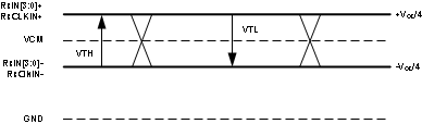 Figure 1. FPD-Link DC VTH/VTL Definition
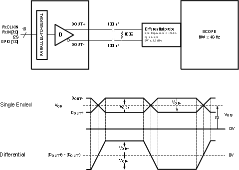 Figure 2. Serializer VOD DC Output
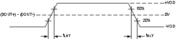 Figure 3. Output Transition Times
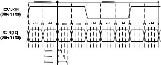 Figure 4. FPD-Link Input Strobe Position
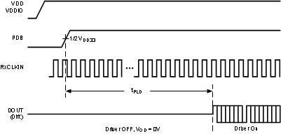 Figure 5. Serializer Lock Time
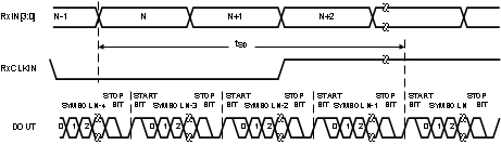 Figure 6. Latency Delay
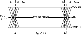 Figure 7. CML Serializer Output Jitter
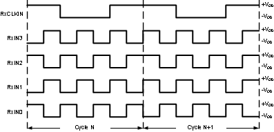 Figure 8. Checkerboard Data Pattern
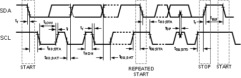 Figure 9. Serial Control Bus Timing Diagram
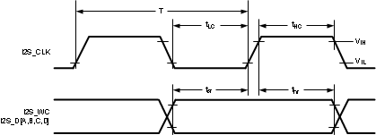 Figure 10. I2S Timing Diagram
6.10 Typical Characteristics
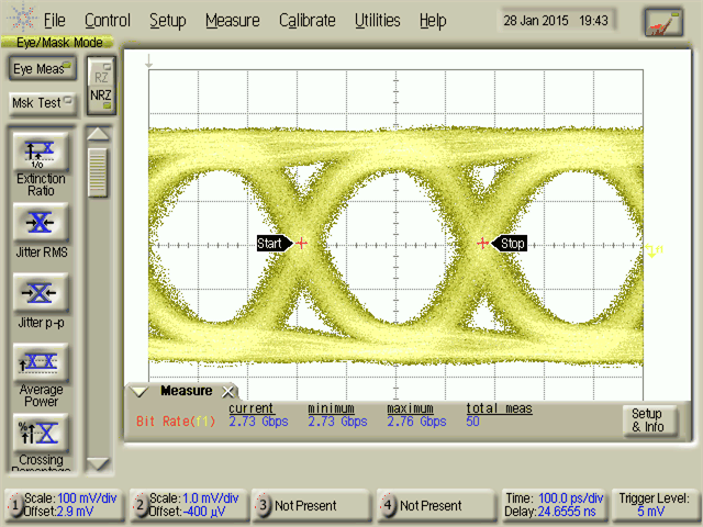 Figure 11. Serializer Eye with 78-MHz Input Clock
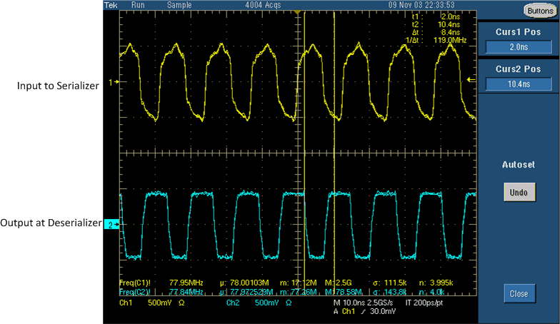 Figure 12. 78-MHz Clock at Serializer and Deserializer