SLASE82B June 2015 – March 2024 HD3SS3411-Q1
PRODUCTION DATA
- 1
- 1 Features
- 2 Applications
- 3 Description
- 4 Pin Configuration and Functions
- 5 Specifications
- 6 Detailed Description
- 7 Application and Implementation
- 8 Device and Documentation Support
- 9 Revision History
- 10Mechanical, Packaging, and Orderable Information
Package Options
Mechanical Data (Package|Pins)
- RWA|14
Thermal pad, mechanical data (Package|Pins)
Orderable Information
7.2.2.1 AC Coupling Capacitors
Many interfaces require AC coupling between the transmitter and receiver. The 0402 capacitors are the preferred option to provide AC coupling, and the 0603 size capacitors will also work. Avoid the 0805 size capacitors and C-packs when possible. Symmetric placement is best for AC coupling capacitors. TI recommends a capacitor value of 0.1μF. Make sure the capacitor value matches the ± signal pair. Make sure the placement is along the TX pairs on the system board, which are usually routed on the top layer of the board.
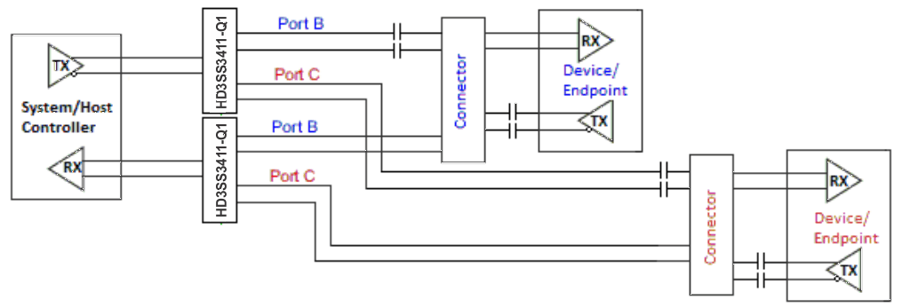
There are several placement options for the AC coupling capacitors. Because the switch requires a bias voltage, the capacitors must only be placed on one side of the switch. If the capacitors are placed on both sides of the switch, make sure to provide a biasing voltage. In Figure 7-2, the coupling capacitors are placed between the switch and endpoint. In this situation, the switch is biased by the system/host controller.
 Figure 7-2 AC Coupling Capacitors Between Switch TX and Endpoint TX
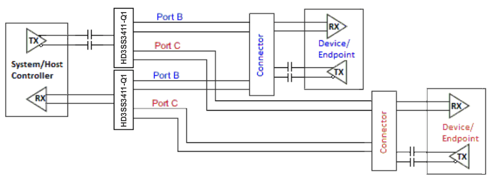
In Figure 7-3, the coupling capacitors are placed on the host transmit pair and endpoint transmit pair. In this situation, the switch on the top is biased by the endpoint and the lower switch is biased by the host controller.
 Figure 7-3 AC Coupling Capacitors on Host TX and Endpoint TX
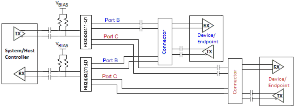
If the common-mode voltage in the system is higher than 2V, the coupling capacitors are placed on both sides of the switch (shown in Figure 7-4). A biasing voltage of less than 2V is required in this case.
 Figure 7-4 AC Coupling Capacitors on Both Sides of Switch