SLAS840C March 2012 – October 2015 HD3SS3415
PRODUCTION DATA.
- 1 Features
- 2 Applications
- 3 Description
- 4 Revision History
- 5 Description continued
- 6 Pin Configuration and Functions
- 7 Specifications
- 8 Parameter Measurement Information
- 9 Detailed Description
- 10Application and Implementation
- 11Power Supply Recommendations
- 12Layout
- 13Device and Documentation Support
- 14Mechanical, Packaging, and Orderable Information
Package Options
Mechanical Data (Package|Pins)
- RUA|42
Thermal pad, mechanical data (Package|Pins)
- RUA|42
Orderable Information
9 Detailed Description
9.1 Overview
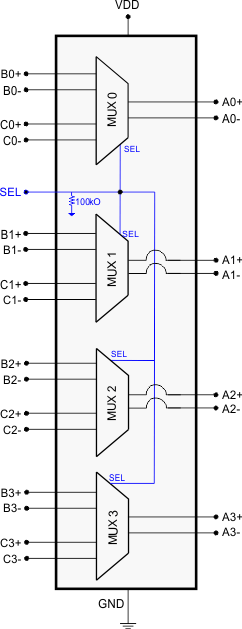
The HD3SS3415 is a high-speed passive switch offered in an industry standard 42-pin WQFN package available in a common footprint shared by several other vendors. The device is specified to operate from a single supply voltage of 3.3 V over the full industrial temperature range of 0°C to 70°C. The HD3SS3415 is a generic 4-CH high-speed mux/demux type of switch that can be used for routing high-speed signals between two different locations on a circuit board. Although it was designed specifically to address PCI Express Gen III applications, the HD3SS3415 will also support several other high-speed data protocols with a differential amplitude of < 1800 mVpp and a common-mode voltage of < 2.0 V, as with USB 3.0 and DisplayPort 1.2.
9.2 Functional Block Diagram

9.3 Feature Description
The HD3SS3415 has a single control line (SEL Pin) which can be used to control the signal path between Port A and either Port B or Port C. Theone select input (SEL) pin of the device can easily be controlled by an available GPIO pin within a system or from a microcontroller.
Table 1. MUX Pin Connections(1)
| PORT A CHANNEL | PORT B OR PORT C CHANNEL CONNECTED TO PORT A CHANNEL |
|
|---|---|---|
| SEL = L | SEL = H | |
| A0+ | B0+ | C0+ |
| A0– | B0– | C0– |
| A1+ | B1+ | C1+ |
| A1– | B1– | C1– |
| A2+ | B2+ | C2+ |
| A2– | B2– | C2– |
| A3+ | B3+ | C3+ |
| A3– | B3– | C3– |
9.4 Device Functional Modes
Table 2 lists the functional modes for the HD3SS3415.
Table 2. HD3SS3415 Control Logic
| CONTROL PIN (SEL) | PORT A TO PORT B CONNECTION STATUS | PORT A TO PORT C CONNECTION STATUS |
|---|---|---|
| L (Default State) | Connected | Disconnected |
| H | Disconnected | Connected |