SNAS649B October   2014  – December 2015 HDC1008

PRODUCTION DATA.  

  1. Features
  2. Applications
  3. Description
  4. Typical Application
  5. Revision History
  6. Pin Configuration and Functions
  7. Specifications
    1. 7.1 Absolute Maximum Ratings
    2. 7.2 ESD Ratings
    3. 7.3 Recommended Operating Conditions
    4. 7.4 Thermal Information
    5. 7.5 Electrical Characteristics
    6. 7.6 I2C Interface Electrical Characteristics
    7. 7.7 I2C Interface Timing Requirements
    8. 7.8 Typical Characteristics
  8. Detailed Description
    1. 8.1 Overview
    2. 8.2 Functional Block Diagram
    3. 8.3 Feature Description
      1. 8.3.1 Power Consumption
      2. 8.3.2 Voltage Supply Monitoring
      3. 8.3.3 Heater
    4. 8.4 Device Functional Modes
    5. 8.5 Programming
      1. 8.5.1 I2C Serial Bus Address Configuration
      2. 8.5.2 I2C Interface
        1. 8.5.2.1 Serial Bus Address
        2. 8.5.2.2 Read and Write Operations
        3. 8.5.2.3 Device Measurement Configuration
    6. 8.6 Register Map
      1. 8.6.1 Temperature Register
      2. 8.6.2 Humidity Register
      3. 8.6.3 Configuration Register
      4. 8.6.4 Serial Number Registers
  9. Application and Implementation
    1. 9.1 Application Information
    2. 9.2 Typical Application
      1. 9.2.1 Design Requirements
      2. 9.2.2 Detailed Design Procedure
      3. 9.2.3 Application Curve
    3. 9.3 Do's and Don'ts
      1. 9.3.1 Soldering
      2. 9.3.2 Hydration Procedure
      3. 9.3.3 Chemical Exposure
  10. 10Power Supply Recommendations
  11. 11Layout
    1. 11.1 Layout Guidelines
      1. 11.1.1 Surface Mount
      2. 11.1.2 Stencil Printing Process
    2. 11.2 Layout Example
  12. 12Device and Documentation Support
    1. 12.1 Documentation Support
      1. 12.1.1 Related Documentation
    2. 12.2 Community Resources
    3. 12.3 Trademarks
    4. 12.4 Electrostatic Discharge Caution
    5. 12.5 Glossary
  13. 13Mechanical, Packaging, and Orderable Information

Package Options

Mechanical Data (Package|Pins)
Thermal pad, mechanical data (Package|Pins)
Orderable Information

6 Pin Configuration and Functions

WLCSP (DSBGA)
8 Pin YPA
Top View
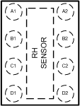
HDC1008 PINOUT.gif

Pin Functions

PIN I/O TYPE(1) DESCRIPTION
NAME NO.
SCL A1 I Serial clock line for I2C, open-drain; requires a pull-up resistor to VDD
VDD B1 P Supply Voltage
ADR0 C1 I Address select pin – hardwired to GND or VDD
ADR1 D1 I Address select pin – hardwired to GND or VDD
SDA A2 I/O Serial data line for I2C, open-drain; requires a pull-up resistor to VDD
GND B2 G Ground
DNC C2 - Do Not Connect, or may be connected to GND
DRDYn D2 O Data ready, active low, open-drain, requires a pull-up resistor to VDD. If not used tie to GND.
(1) P=Power, G=Ground, I=Input, O=Output