SLLSEC4B June 2013 – August 2016 HVDA551-Q1 , HVDA553-Q1
PRODUCTION DATA.
- 1 Features
- 2 Applications
- 3 Description
- 4 Revision History
- 5 Pin Configuration and Functions
- 6 Specifications
- 7 Parameter Measurement Information
- 8 Detailed Description
- 9 Application and Implementation
- 10Power Supply Recommendations
- 11Layout
- 12Device and Documentation Support
- 13Mechanical, Packaging, and Orderable Information
Package Options
Mechanical Data (Package|Pins)
- D|8
Thermal pad, mechanical data (Package|Pins)
Orderable Information
1 Features
- Qualified for Automotive Applications
- AEC-Q100 Qualified With the Following Results:
- Device Temperature Grade 1: –40°C to +125°C Ambient Operating Temperature
- Device HBM ESD Classification Level:
- Level 3B for Pins 6 and 7
- Level 3A for All Other Pins
- Device CDM ESD Classification Level C6
- Meets or Exceeds the Requirements of ISO 11898-2 and ISO 11898-5
- GIFT/ICT Compliant
- Data Rate Up to 1 Mbps
- ESD Protection Up to ±12 kV (Human-Body Model) on Bus Pins
- I/O Voltage Level Adapting
- HVDA551: Adaptable I/O Voltage Range (VIO) From 3 V to 5.33 V
- SPLIT Voltage Source
- HVDA553: Common-Mode Bus Stabilization
- Operating Modes:
- Normal Mode
- Low-Power Standby Mode With RXD Wake-Up Request
- High Electromagnetic Compliance (EMC)
- Supports CAN Flexible Data-Rate (FD)
- Protection
- Undervoltage Protection on VIO and VCC
- Bus-Fault Protection of –27 V to 40 V
- TXD Dominant State Time-Out
- RXD Wake-Up Request Lockout on CAN Bus Stuck Dominant Fault (HVDA551)
- Digital Inputs Compatible With 5-V Microprocessors (HVDA553)
- Thermal Shutdown Protection
- Power-Up and Power-Down Glitch-Free Bus I/O
- High Bus Input Impedance When Unpowered (No Bus Load)
2 Applications
- SAE J2284 High-Speed CAN for Automotive Applications
- SAE J1939 Standard Data Bus Interface
- GMW3122 Dual-Wire CAN Physical Layers
- ISO 11783 Standard Data Bus Interface
- NMEA 2000 Standard Data Bus Interface
3 Description
The HVDA55x-Q1 device is designed and qualified for use in automotive applications and meets or exceeds the specifications of the ISO 11898 High Speed CAN (Controller Area Network) Physical Layer standard (transceiver).
Device Information(1)
| PART NUMBER | PACKAGE | BODY SIZE (NOM) |
|---|---|---|
| HVDA551-Q1 HVDA553-Q1 |
SOIC (8) | 4.90 mm × 3.91 mm |
- For all available packages, see the orderable addendum at the end of the data sheet.
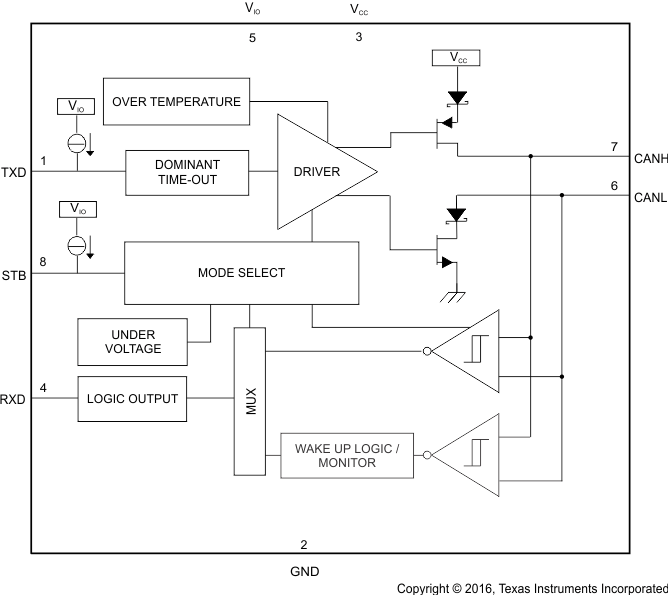
HVDA551 Block Diagram

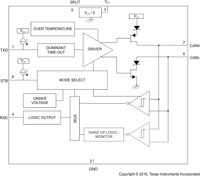
HVDA553 Block Diagram
