SLLSEC4B June 2013 – August 2016 HVDA551-Q1 , HVDA553-Q1
PRODUCTION DATA.
- 1 Features
- 2 Applications
- 3 Description
- 4 Revision History
- 5 Pin Configuration and Functions
- 6 Specifications
- 7 Parameter Measurement Information
- 8 Detailed Description
- 9 Application and Implementation
- 10Power Supply Recommendations
- 11Layout
- 12Device and Documentation Support
- 13Mechanical, Packaging, and Orderable Information
Package Options
Mechanical Data (Package|Pins)
- D|8
Thermal pad, mechanical data (Package|Pins)
Orderable Information
8 Detailed Description
8.1 Overview
The device meets or exceeds the specifications of the ISO 11898 High-Speed CAN (Controller Area Network) Physical Layer standard (transceiver). This device provides CAN transceiver functions: differential transmit capability to the bus and differential receive capability at data rates up to 1 megabit per second (Mbps). The device includes many protection features providing device and CAN network robustness.
8.2 Functional Block Diagrams
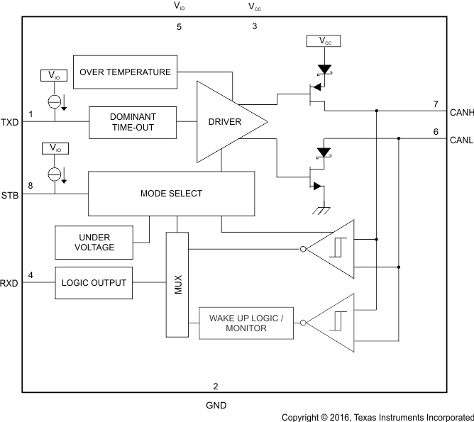 Figure 13. HVDA551 Block Diagram
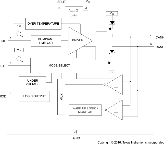 Figure 14. HVDA553 Block Diagram
8.3 Feature Description
8.3.1 Digital Inputs and Outputs
The HVDA551 device has an I/O supply voltage input pin (VIO) to ratiometrically level shift the digital logic input and output levels with respect to VIO for compatibility with protocol controllers having I/O supply voltages between 3 V and 5.33 V.
The HVDA553 devices have a single VCC supply (5 V). The digital logic input and output levels for these devices are with respect to VCC for compatibility with protocol controllers having I/O supply voltages between 4.68 V and 5.33 V.
8.3.2 Using the HVDA553 With Split Termination
The SPLIT pin voltage output provides 0.5 × VCC in normal mode. The circuit may be used by the application to stabilize the common-mode voltage of the bus by connecting it to the center tap of split termination for the CAN network (see Figure 15 and Figure 23). This pin provides a stabilizing recessive voltage drive to offset leakage currents of unpowered transceivers or other bias imbalances that might bring the network common-mode voltage away from 0.5 × VCC. Using this feature in a CAN network improves electromagnetic emissions behavior of the network by eliminating fluctuations in the bus common-mode voltage levels at the start of message transmissions.
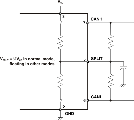 Figure 15. SPLIT Pin Circuitry and Application
8.3.3 Protection Features
8.3.3.1 TXD Dominant State Time Out
During normal mode, the only mode where the CAN driver is active, the TXD dominant time-out circuit prevents the transceiver from blocking network communication in the event of a hardware or software failure where TXD is held dominant longer than the time-out period t(DOM). The dominant time-out circuit is triggered by a falling edge on TXD. If no rising edge is seen before the time-out constant of the circuit expires (t(DOM)) the CAN bus driver is disabled, freeing the bus for communication between other network nodes. The CAN driver is re-activated when a recessive signal is seen on the TXD pin, thus clearing the dominant-state time-out. The CAN bus pins are biased to the recessive level during a TXD dominant-state time-out.
NOTE
The maximum dominant TXD time allowed by the TXD dominant-state time-out limits the minimum possible data rate of the devices.
The CAN protocol allows a maximum of eleven successive dominant bits (on TXD) for the worst case, where five successive dominant bits are followed immediately by an error frame. This, along with the t(DOM) minimum, limits the minimum bit rate. The minimum bit rate may be calculated by Equation 1:
8.3.3.2 Thermal Shutdown
If the junction temperature of the device exceeds the thermal shutdown threshold, the device turns off the CAN driver circuits. This condition is cleared once the temperature drops below the thermal shutdown temperature of the device. The CAN bus pins are biased to the recessive level during a thermal shutdown.
8.3.3.3 Undervoltage Lockout or Unpowered Device
Both of the supply pins have undervoltage detection, which places the device in forced standby mode to protect the bus during an undervoltage event on either the VCC or VIO supply pins. If VIO is undervoltage, the RXD pin is forced to the high-impedance state and the device does not pass any wake-up signals from the bus to the RXD pin. Because the device is placed into forced standby mode, the CAN bus pins have a common-mode bias to ground, protecting the CAN network; see Figure 16 and Figure 17.
The device is designed to be an ideal passive load to the CAN bus if it is unpowered. The bus pins (CANH, CANL) have extremely low leakage currents when the device is unpowered, so they do not load down the bus but rather be a no-load. This is critical, especially if some nodes of the network are unpowered while the rest of the network remains in operation.
NOTE
Once an undervoltage condition is cleared and VCC and VIO have returned to valid levels, the device typically requires 300 µs to transition to normal operation.
Table 2. Undervoltage Protection
| DEVICE | VCC | VIO | DEVICE STATE | BUS | RXD |
|---|---|---|---|---|---|
| Both devices | Bad | Good | Forced standby mode | Common mode bias to GND(1) | Mirrors bus state through wake-up filter(2) |
| Good | Bad | Forced standby mode(3) | Common mode bias to GND(1) | High Z | |
| Unpowered | Unpowered | No load | High Z | ||
8.3.3.4 Floating Pins
The device has integrated pullups and pulldowns on critical pins to place the device into known states if the pins float. The TXD and STB pins on the HVDA551 are pulled up to VIO. This forces a recessive input level on TXD in the case of a floating TXD pin and prevents the device from entering into the low-power standby mode if the STB pin floats. In the case of the HVDA553 both the TXD and STB pins are pulled up to VCC, which has the same effect.
8.3.3.5 CAN Bus Short-Circuit Current Limiting
The device has several protection features that limit the short-circuit current when a CAN bus line is shorted. These include CAN driver-current limiting (dominant and recessive) and TXD dominant-state time-out to prevent continuously driving dominant. During CAN communication, the bus switches between dominant and recessive states; thus, the short-circuit current may be viewed either as the current during each bus state or as a DC average current. For system current and power considerations in termination resistance and common-mode choke ratings, the average short-circuit current must be used. The device has TXD dominant-state time-out, which prevents permanently having the higher short-circuit current of dominant state. The CAN protocol also has forced state changes and recessive bits such as bit stuffing, control fields, and interframe space. These ensure there is a minimum recessive amount of time on the bus even if the data field contains a high percentage of dominant bits.
NOTE
The short-circuit current of the bus depends on the ratio of recessive to dominant bits and their respective short-circuit currents.
The average short-circuit current may be calculated with Equation 2:
where
- IOS(AVG) is the average short-circuit current
- %Transmit is the percentage the node is transmitting CAN messages
- %Receive is the percentage the node is receiving CAN messages
- %REC_Bits is the percentage of recessive bits in the transmitted CAN messages
- %DOM_Bits is the percentage of dominant bits in the transmitted CAN messages
- IOS(SS)_REC is the recessive steady-state, short-circuit current
- IOS(SS)_DOM is the dominant steady-state, short-circuit current
8.4 Device Functional Modes
These devices have two main operating modes: normal mode and standby mode. Table 3 lists these modes in detail. Operating mode selection is made through the STB input pin.
Table 3. Operating Modes
| DEVICE | STB | MODE | DRIVER | RECEIVER | RXD Pin |
|---|---|---|---|---|---|
| All devices | LOW | Normal mode | Enabled (On) | Enabled (On) | Mirrors bus state(1) |
| HIGH | Standby mode (RXD wake-up request) | Disabled (Off) | Low-power wake-up receiver and bus monitor enabled | Mirrors bus state through wake-up filter(2) |
8.4.1 Bus States by Mode
The CAN bus has three valid states during powered operation, depending on the mode of the device. In normal mode, the bus may be dominant (logic LOW) where the bus lines are driven differentially apart, or or the bus may be recessive (logic HIGH) where the bus lines are biased to VCC / 2 through the high-ohmic internal input resistors RIN of the receiver. The third state is low-power standby mode where the bus lines are biased to GND through the high-ohmic internal input resistors RIN of the receiver.
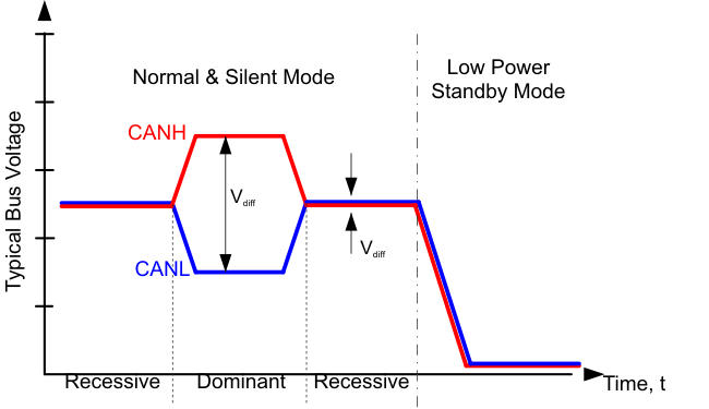 Figure 16. Bus States (Physical Bit Representation)
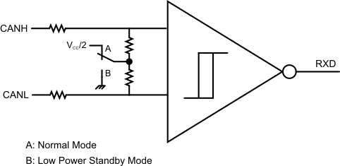 Figure 17. Simplified Common-Mode Bias and Receiver Implementation
8.4.2 Normal Mode
This is the normal operating mode of the device. Normal mode is selected by setting STB low. The CAN driver and receiver are fully operational and CAN communication is bidirectional. The driver is translating a digital input on TXD to a differential output on CANH and CANL. The receiver is translating the differential signal from CANH and CANL to a digital output on RXD. In recessive state, the CAN bus pins (CANH and CANL) are biased to 0.5 × VCC. In dominant state, the bus pins are driven differentially apart. Logic high is equivalent to recessive on the bus, and logic low is equivalent to a dominant (differential) signal on the bus.
8.4.3 Standby Mode With RXD Wake-Up Request
This is the low-power mode of the device. Standby mode is selected by setting STB high. The CAN driver and main receiver are turned off and bidirectional CAN communication is not possible. The low-power receiver and bus monitor, both supplied through the VIO supply, are enabled to allow for RXD wake-up requests through the CAN bus. The VCC (5-V) supply may be turned off for additional power savings at the system level. A wake-up request is output to RXD (driven low) for any dominant bus transmissions longer than the filter time tBUS. The local protocol controller (MCU) must monitor RXD for transitions and then reactivate the device to normal mode based on the wake-up request. The 5-V (VCC) supply must be reactivated by the local protocol controller to resume normal mode if it has been turned off for low-power standby operation. The CAN bus pins are weakly pulled to GND, see Figure 16 and Figure 17.
8.4.3.1 RXD Wake-Up Request Lockout for Bus-Stuck Dominant Fault (HVDA551)
If the bus has a fault condition where it is stuck dominant while the HVDA551 is placed into standby mode through the STB pin, the device locks out the RXD wake-up request until the fault has been removed to prevent false wake-up signals in the system.
 Figure 18. HVDA551 RXD Wake-Up Request With No Bus Fault Condition
 Figure 19. HVDA551 RXD Wake-Up Request Lockout During Bus Dominant Fault Condition
8.4.4 Driver and Receiver Function Tables
Table 4 shows the behavior of devices when in driver mode.
Table 4. Driver Function Table
| DEVICE | INPUTS | OUTPUTS | DRIVEN BUS STATE | ||
|---|---|---|---|---|---|
| STB / S(1) | TXD(1) | CANH(1) | CANL(1) | ||
| Both devices | L | L | H | L | Dominant |
| L | H | Z | Z | Recessive | |
| L | Open | Z | Z | Recessive | |
| HVDA551, HVDA553(2) | H | X | Y | Y | Recessive |
Table 5. Receiver Function Table
| DEVICE MODE | CAN DIFFERENTIAL INPUTS VID = V(CANH) – V(CANL) |
BUS STATE | RXD PIN(1) | |
|---|---|---|---|---|
| Standby with RXD wake-up request (HVDA551, HVDA553)(2) | VID ≥ 1.15 V | DOMINANT | L | |
| 0.4 V < VID < 1.15 V | ? | ? | ||
| VID ≤ 0.4 V | RECESSIVE | H | ||
| NORMAL | VID ≥ 0.9 V | DOMINANT | L | |
| 0.5 V < VID < 0.9 V | ? | ? | ||
| VID ≤ 0.5 V | RECESSIVE | H | ||
| ANY | Open | N/A | H | |