SBOS818B December 2016 – November 2018 INA1650 , INA1651
PRODUCTION DATA.
- 1 Features
- 2 Applications
- 3 Description
- 4 Revision History
- 5 Pin Configuration and Functions
- 6 Specifications
- 7 Detailed Description
-
8 Application and Implementation
- 8.1 Application Information
- 8.2
Typical Applications
- 8.2.1 Line Receiver for Differential Audio Signals in a Split-Supply System
- 8.2.2 Differential Line Receiver for Single-Supply Applications
- 8.2.3 Floating Single-Ended Input Line Receiver for Ground Loop Noise Reduction
- 8.2.4 Floating Single-Ended Input Line Receiver With Differential Outputs
- 8.2.5 TRS Audio Interface in Single-Supply Applications
- 8.2.6 Differential Line Driver With Single-Ended Input
- 9 Power Supply Recommendations
- 10Layout
- 11Device and Documentation Support
- 12Mechanical, Packaging, and Orderable Information
Package Options
Mechanical Data (Package|Pins)
- PW|14
Thermal pad, mechanical data (Package|Pins)
- PW|14
Orderable Information
7.3.2 Supply Divider
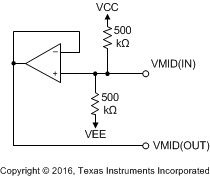
The INA165x integrates a supply-divider circuit which may bias the input common-mode voltage and output reference voltage to the halfway point between the applied power supply voltages. The nominal output voltage of the supply divider circuit is shown in Equation 2:

Figure 40 illustrates the internal topology of the supply-divider circuit. The supply divider consists of two 500-kΩ resistors connected between the VCC and VEE pins of the INA165x. The noninverting input of a buffer amplifier is connected to the midpoint of the voltage divider that is formed by the 500-kΩ resistors. The buffer amplifier provides a low-impedance output that is required to bias the REF pins without degrading the CMRR. For dual-supply applications where the supply divider circuit may not be used, no connection is required for the VMID(IN) or VMID(OUT) pins.
 Figure 40. Internal Supply Divider Circuit