SBOSA08 February 2021 INA183
PRODUCTION DATA
- 1 Features
- 2 Applications
- 3 Description
- 4 Revision History
- 5 Device Comparison
- 6 Pin Configuration and Functions
- 7 Specifications
- 8 Detailed Description
- 9 Application and Implementation
- 10Power Supply Recommendations
- 11Layout
- 12Device and Documentation Support
- 13Mechanical, Packaging, and Orderable Information
Package Options
Mechanical Data (Package|Pins)
- DBV|5
Thermal pad, mechanical data (Package|Pins)
Orderable Information
9.1.1 RSENSE and Device Gain Selection
Choosing the largest possible shunt resistor will maximize the accuracy of any current-sense amplifier. A large sense resistor maximizes the differential input signal for a given amount of current flow and reduces the error contribution of the offset voltage. However, there are practical limits as to how large the current-sense resistor can be in a given application because of the resistor size and maximum allowable power dissipation. Equation 1 gives the maximum value for the current-sense resistor for a given power dissipation budget:
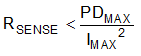
where:
- PDMAX is the maximum allowable power dissipation in RSENSE.
- IMAX is the maximum current expected to flow through RSENSE.
An additional limitation on the size of the current-sense resistor and device gain is due to the power-supply voltage at the IN+ pin, and device swing-to-rail limitations. To ensure that the current-sense signal is properly passed to the output, both positive and negative output swing limitations must be examined. Equation 2 provides the maximum values of RSENSE and GAIN to keep the device from exceeding the positive swing limitation.
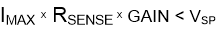
where:
- IMAX is the maximum current that will flow through RSENSE.
- GAIN is the gain of the current-sense amplifier.
- VSP is the positive output swing as specified in the data sheet.
Positive output swing limitations should be considered when selecting the value of RSENSE. There is always a trade-off between the value of the sense resistor and the gain of the device under consideration. If the sense resistor selected for the maximum power dissipation is too large, then it is possible to select a lower-gain device to avoid positive swing limitations.
The negative swing specification limits how small the sense resistor value can be for a given application. Equation 3 provides the limit on the minimum value of the sense resistor.
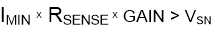
where:
- IMIN is the minimum current that will flow through RSENSE.
- GAIN is the gain of the current-sense amplifier.
- VSN is the negative output swing of the device.