SBOS307G May 2004 – January 2015 INA193 , INA194 , INA195 , INA196 , INA197 , INA198
PRODUCTION DATA.
- 1 Features
- 2 Applications
- 3 Description
- 4 Revision History
- 5 Device Comparison Table
- 6 Pin Configuration and Functions
- 7 Specifications
- 8 Detailed Description
- 9 Application and Implementation
- 10Power Supply Recommendations
- 11Layout
- 12Device and Documentation Support
- 13Mechanical, Packaging, and Orderable Information
Package Options
Mechanical Data (Package|Pins)
- DBV|5
Thermal pad, mechanical data (Package|Pins)
Orderable Information
11 Layout
11.1 Layout Guidelines
11.1.1 RFI and EMI
Attention to good layout practices is always recommended. Keep traces short and, when possible, use a printed circuit board (PCB) ground plane with surface-mount components placed as close to the device pins as possible. Small ceramic capacitors placed directly across amplifier inputs can reduce RFI/EMI sensitivity. PCB layout should locate the amplifier as far away as possible from RFI sources. Sources can include other components in the same system as the amplifier itself, such as inductors (particularly switched inductors handling a lot of current and at high frequencies). RFI can generally be identified as a variation in offset voltage or DC signal levels with changes in the interfering RF signal. If the amplifier cannot be located away from sources of radiation, shielding may be needed. Twisting wire input leads makes them more resistant to RF fields. The difference in input pin location of the INA193-INA195 devices versus the INA196-INA198 devices may provide different EMI performance.
11.2 Layout Example
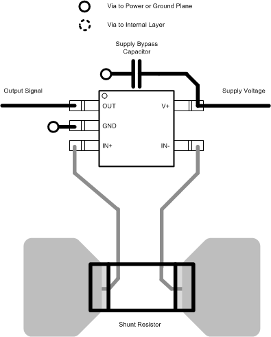
 Figure 31. Recommended Layout