SBOS307G May   2004  – January 2015 INA193 , INA194 , INA195 , INA196 , INA197 , INA198

PRODUCTION DATA.  

  1. Features
  2. Applications
  3. Description
  4. Revision History
  5. Device Comparison Table
  6. Pin Configuration and Functions
  7. Specifications
    1. 7.1 Absolute Maximum Ratings
    2. 7.2 ESD Ratings
    3. 7.3 Recommended Operating Conditions
    4. 7.4 Thermal Information
    5. 7.5 Electrical Characteristics
    6. 7.6 Typical Characteristics
  8. Detailed Description
    1. 8.1 Overview
    2. 8.2 Functional Block Diagram
    3. 8.3 Feature Description
      1. 8.3.1 Basic Connection
      2. 8.3.2 Selecting RS
      3. 8.3.3 Inside the INA193-INA198
    4. 8.4 Device Functional Modes
      1. 8.4.1 Input Filtering
      2. 8.4.2 Accuracy Variations as a Result of VSENSE and Common-Mode Voltage
        1. 8.4.2.1 Normal Case 1: VSENSE ≥ 20mv, VCM ≥ VS
        2. 8.4.2.2 Normal Case 2: VSENSE ≥ 20mv, VCM < VS
        3. 8.4.2.3 Low VSENSE Case 1: VSENSE < 20mV, −16v ≤ VCM < 0; and Low VSENSE Case 3: VSENSE < 20mV, VS < VCM ≤ 80V
        4. 8.4.2.4 Low VSENSE Case 2: VSENSE < 20 mV, 0 V ≤ VCM ≤ VS
      3. 8.4.3 Shutdown
      4. 8.4.4 Transient Protection
      5. 8.4.5 Output Voltage Range
  9. Application and Implementation
    1. 9.1 Application Information
    2. 9.2 Typical Application
      1. 9.2.1 Design Requirements
      2. 9.2.2 Detailed Design Procedure
      3. 9.2.3 Application Curve
  10. 10Power Supply Recommendations
  11. 11Layout
    1. 11.1 Layout Guidelines
      1. 11.1.1 RFI and EMI
    2. 11.2 Layout Example
  12. 12Device and Documentation Support
    1. 12.1 Related Links
    2. 12.2 Trademarks
    3. 12.3 Electrostatic Discharge Caution
    4. 12.4 Glossary
  13. 13Mechanical, Packaging, and Orderable Information

Package Options

Mechanical Data (Package|Pins)
Thermal pad, mechanical data (Package|Pins)
Orderable Information

Pin Configuration and Functions

DBV Package
5-Pin SOT-23
INA193, INA194, INA195 Top View
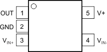
INA193 INA194 INA195 INA196 INA197 INA198 po_193-195_bos307.gif
DBV Package
5-Pin SOT-23
INA196, INA197, INA198 Top View
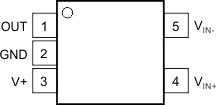
INA193 INA194 INA195 INA196 INA197 INA198 po_196-198_bos307.gif

Pin Functions

PIN TYPE DESCRIPTION
NAME INA193,
INA194,
INA195
INA196,
INA197,
INA198
DBV DBV
GND 2 2 GND Ground
OUT 1 1 O Output voltage
V+ 5 3 Analog Power supply, 2.7 V to 18 V
VIN+ 3 4 I Connect to supply side of shunt resistor
VIN– 4 5 I Connect to load side of shunt resistor