SBOS558D April 2011 – April 2025 INA200-Q1 , INA201-Q1 , INA202-Q1
PRODUCTION DATA
- 1
- 1 Features
- 2 Applications
- 3 Description
- 4 Device Comparison
- 5 Pin Configuration and Functions
- 6 Specifications
- 7 Parameter Measurement Information
- 8 Detailed Description
- 9 Application Information
- 10Device and Documentation Support
- 11Revision History
- 12Mechanical, Packaging, and Orderable Information
Package Options
Mechanical Data (Package|Pins)
- DGK|8
Thermal pad, mechanical data (Package|Pins)
Orderable Information
9.1.3 Input Filtering
An obvious and straightforward location for filtering is at the output of the INA20x-Q1 series; however, this location negates the advantage of the low output impedance of the internal buffer. The only other option for filtering is at the input pins of the INA20x-Q1, but the internal 5-kΩ + 30% input impedance complicates input filtering, as illustrated in Figure 9-2. Use the lowest possible resistor values to minimize both the initial shift in gain and effects of tolerance. Equation 1 gives the effect on initial gain:
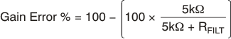
 Figure 9-2 Input Filter
To calculate the total effect on gain error, replace the 5-kΩ term with 5 kΩ – 30%, (or 3.5 kΩ) or 5 kΩ + 30% (or 6.5 kΩ). One can also be insert the tolerance extremes of RFILT into the equation. If using a pair of 100-Ω 1% resistors on the inputs, the initial gain error is 1.96%. Worst-case tolerance conditions always occur at the lower excursion of the internal 5-kΩ resistor (3.5-kΩ), and the higher excursion of RFILT + 3% in this case.
Note that one must then combine the specified accuracy of the INA20x-Q1 in addition to these tolerances. Although this discussion treated worst-case accuracy conditions by combining the extremes of the resistor values, it is appropriate to use geometric-mean or root-sum-square calculations to total the effects of accuracy variations.