SBOS374E November 2006 – September 2017 INA200 , INA201 , INA202
PRODUCTION DATA.
- 1 Features
- 2 Applications
- 3 Description
- 4 Revision History
- 5 Pin Configuration and Functions
- 6 Specifications
- 7 Detailed Description
- 8 Application and Implementation
- 9 Power Supply Recommendations
- 10Layout
- 11Device and Documentation Support
- 12Mechanical, Packaging, and Orderable Information
Package Options
Mechanical Data (Package|Pins)
Thermal pad, mechanical data (Package|Pins)
Orderable Information
9 Power Supply Recommendations
The input circuitry of the INA20x devices can accurately measure beyond the power-supply voltage, Vs. For example, the Vs power supply is 5 V, whereas the load power-supply voltage is up to 80 V. However, the output voltage range of the OUT pin is limited by the voltages on the power supply pin.
9.1 Output vs Supply Ramp Considerations
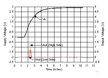
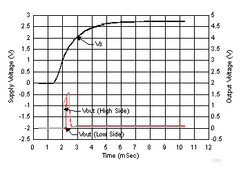
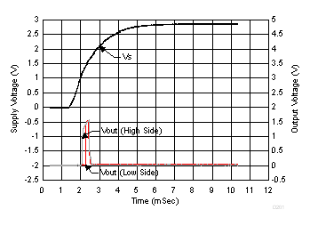
Figure 36, Figure 37, and Figure 38 show the typical output voltages for high and low-side configurations with the given ramp supply voltage. These fluctuations on the output during power-up may require a controller to incorporate a blanking time to disregard the artifacts.
 Figure 36. Analog Output vs Supply Ramp (INA200)
 Figure 38. Analog Output vs Supply Ramp (INA202)
 Figure 37. Analog Output vs Supply Ramp (INA201)