SBOS728A February   2015  – March 2021 INA225-Q1

PRODUCTION DATA  

  1. Features
  2. Applications
  3. Description
  4. Revision History
  5. Pin Configuration and Functions
  6. Specifications
    1. 6.1 Absolute Maximum Ratings (1)
    2. 6.2 ESD Ratings
    3. 6.3 Recommended Operating Conditions
    4. 6.4 Thermal Information
    5. 6.5 Electrical Characteristics
    6. 6.6 Typical Characteristics
  7. Detailed Description
    1. 7.1 Overview
    2. 7.2 Functional Block Diagram
    3. 7.3 Feature Description
      1. 7.3.1 Selecting A Shunt Resistor
        1. 7.3.1.1 Selecting A Current-Sense Resistor Example
        2. 7.3.1.2 Optimizing Power Dissipation versus Measurement Accuracy
      2. 7.3.2 Programmable Gain Select
    4. 7.4 Device Functional Modes
      1. 7.4.1 Input Filtering
      2. 7.4.2 Shutting Down the Device
      3. 7.4.3 Using the Device with Common-Mode Transients Above 36 V
  8. Applications and Implementation
    1. 8.1 Application Information
    2. 8.2 Typical Applications
      1. 8.2.1 Microcontroller-Configured Gain Selection
        1. 8.2.1.1 Design Requirements
        2. 8.2.1.2 Detailed Design Procedure
        3. 8.2.1.3 Application Curve
      2. 8.2.2 Unidirectional Operation
        1. 8.2.2.1 Design Requirements
        2. 8.2.2.2 Detailed Design Procedure
        3. 8.2.2.3 Application Curve
      3. 8.2.3 Bidirectional Operation
        1. 8.2.3.1 Design Requirements
        2. 8.2.3.2 Detailed Design Procedure
        3. 8.2.3.3 Application Curve
  9. Power Supply Recommendations
  10. 10Layout
    1. 10.1 Layout Guidelines
    2. 10.2 Layout Example
  11. 11Device and Documentation Support
    1. 11.1 Documentation Support
      1. 11.1.1 Related Documentation
    2. 11.2 Receiving Notification of Documentation Updates
    3. 11.3 Support Resources
    4. 11.4 Trademarks
    5. 11.5 Electrostatic Discharge Caution
    6. 11.6 Glossary
  12. 12Mechanical, Packaging, and Orderable Information

Package Options

Mechanical Data (Package|Pins)
Thermal pad, mechanical data (Package|Pins)
Orderable Information

Typical Characteristics

At TA = +25 °C, VS = +5 V, VIN+ = 12 V, and VREF = VS / 2, unless otherwise noted.
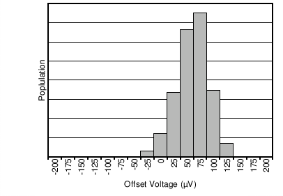
GUID-D1DF6B2C-4C99-4CAD-A0DC-0DB21E6CE84E-low.png


Figure 6-1 Input Offset Voltage Production Distribution
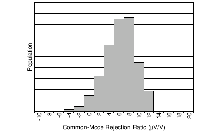
GUID-126DC58E-B9A9-41D3-BD25-C554BAD2A6FC-low.png


Figure 6-3 Common-Mode Rejection Production Distribution
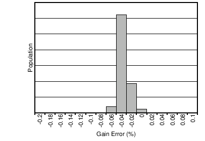
GUID-4D289D41-A7CA-4B37-8434-4A73EB34A847-low.png


Figure 6-5 Gain Error Production Distribution (Gain = 25 V/V)
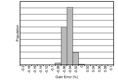
GUID-19BC8298-659B-4CBC-9E14-A233CEA53D2E-low.png


Figure 6-7 Gain Error Production Distribution (Gain = 100 V/V)
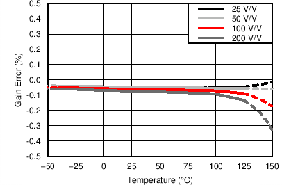
GUID-6B575DD5-5EF6-4A55-B39D-FFF52FED5F2C-low.png


Figure 6-9 Gain Error vs. Temperature
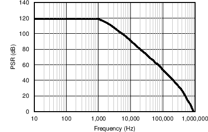
GUID-A7C82CA1-C7BE-4CBD-8CE9-8E126D4A296D-low.png
VCM = 0 VVREF = 2.5 VVSENSE = 0 mV, Shorted
VS = 5 V + 250-mV Sine Disturbance
Figure 6-11 Power-Supply Rejection Ratio vs. Frequency
GUID-1F33F74A-2A67-47BE-9CE7-8E2C070E5020-low.png


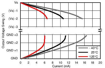
Figure 6-13 Output Voltage Swing vs Output Current
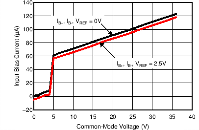
GUID-1B7CBA45-7CE0-4870-8EB7-960B06BE70DB-low.png


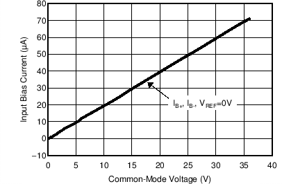
Figure 6-15 Input Bias Current vs. Common-Mode Voltage (Supply Voltage = +5 V)
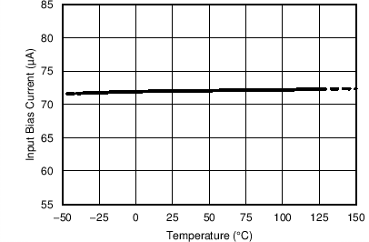
GUID-D32F1EFB-02E8-4EE7-B711-E67F4E357080-low.png
VS = 5 VVCM = 12 V
Figure 6-17 Input Bias Current vs. Temperature
GUID-1AFB79F7-B52C-4784-B024-286BD950EFFC-low.png


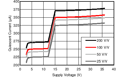
Figure 6-19 Quiescent Current vs. Supply Voltage
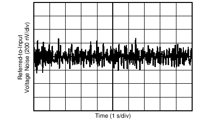
GUID-6FAEC56C-6EFC-401B-AE0F-93E3DF8D98B4-low.png
VS = ± 2.5 VVCM = 0 VVSENSE = 0 mV, Shorted
Figure 6-21 0.1-Hz to 10-Hz Voltage Noise (Referred-to-Input)
GUID-9733F1B3-8A48-418F-B566-18D3E873BF09-low.png


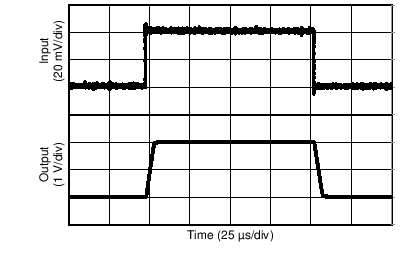
Figure 6-23 Step Response (Gain = 50 V/V, 2-VPP Output Step)
GUID-8CCFDA43-8553-4E27-9018-C66004495A4B-low.png


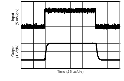
Figure 6-25 Step Response (Gain = 200 V/V, 2-VPP Output Step)
GUID-90A6FD94-C33B-4129-95B5-3022B881306C-low.png
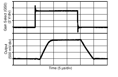
VDIFF = 20 mV VOUT at 25-V/V Gain = 500 mV
VOUT at 100-V/V Gain = 2 V
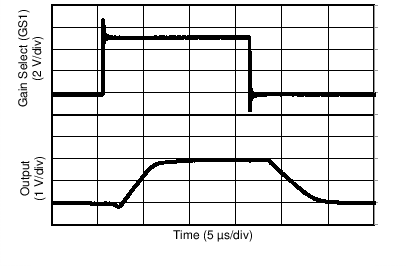
Figure 6-27 Gain Change Output Response (Gain = 25 V/V to 100 V/V)
GUID-116196F8-407D-45D9-9E33-7787386EA96A-low.png
VDIFF = 20 mV VOUT at 100-V/V Gain = 2 V
VOUT at 200-V/V Gain = 4 V
Figure 6-29 Gain Change Output Response (Gain = 100 V/V to 200 V/V)
GUID-5088010D-6836-4F0F-9739-3101354F800E-low.png


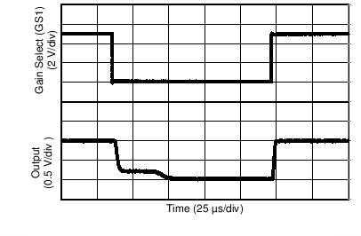
Figure 6-31 Gain Change Output Response From Saturation (Gain = 100 V/V to 25 V/V)
GUID-0788F7CC-F6D2-4534-88EF-F49D41E96DE8-low.png


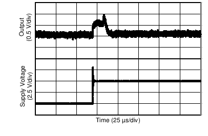
Figure 6-33 Gain Change Output Response From Saturation (Gain = 200 V/V to 100 V/V)
GUID-5C96993D-E301-4DB2-93E3-A81B48F81E9D-low.png


Figure 6-35 Start-Up Response
GUID-8227EEF8-491A-4D5B-B2F7-DC1FCC1D8D45-low.png


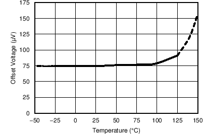
Figure 6-2 Input Offset Voltage vs. Temperature
GUID-167FB749-0B92-40CF-B9D4-478A203EB5D1-low.png


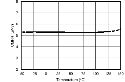
Figure 6-4 Common-Mode Rejection Ratio vs. Temperature
GUID-CD38FC57-6452-4716-80DB-197A107BFC66-low.png


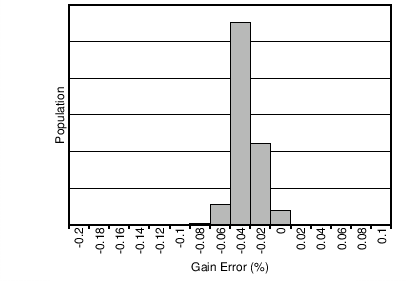
Figure 6-6 Gain Error Production Distribution (Gain = 50 V/V)
GUID-D60CD364-87BE-4BBF-B679-7B51C5463798-low.png


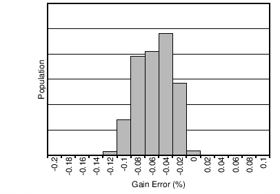
Figure 6-8 Gain Error Production Distribution (Gain = 200 V/V)
GUID-DE7A7B6A-0C0D-49D0-93A0-0653048E889B-low.png
VCM = 0 VVSENSE = 15 mVPP
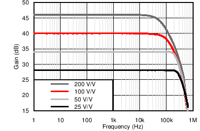
Figure 6-10 Gain vs. Frequency
GUID-5D622EA5-C6F6-48EA-B926-AA9CB608ABDC-low.png
VS = 5 VVREF = 2.5 VVSENSE = 0 mV, Shorted
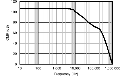
VCM = 1-V Sine Wave
Figure 6-12 Common-Mode Rejection Ratio vs. Frequency
GUID-ECAF8F0B-B0E3-4308-A73B-6C4DCF94F515-low.png
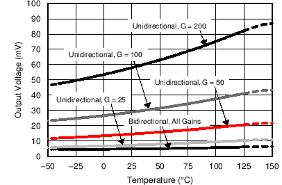
Unidirectional, REF = GNDBidirectional, REF > GND
Figure 6-14 Unidirectional Output Voltage Swing vs. Temperature
GUID-FC1294D2-84F3-4A26-A55B-2F3415F4CE05-low.png


Figure 6-16 Input Bias Current vs. Common-Mode Voltage (Supply Voltage = 0 V, Shutdown)
GUID-7B40BC00-D978-47E8-B0FA-E0C3DF03C298-low.png


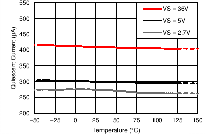
Figure 6-18 Quiescent Current vs. Temperature
GUID-CC9C1563-D759-4BD9-AB04-171D7FAA3C46-low.png
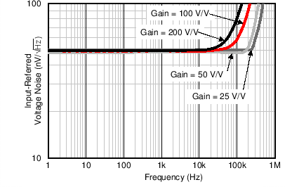
VS = ± 2.5 VVREF = 0 VVSENSE = 0 mV, Shorted
Figure 6-20 Input-Referred Voltage Noise vs. Frequency
GUID-0F1A7862-84A8-425E-8ED0-23E2D082E6CF-low.png


Figure 6-22 Step Response (Gain = 25 V/V, 2-VPP Output Step)
GUID-3D865496-CE71-434F-8940-E7B7F0082B7D-low.png


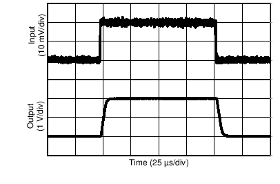
Figure 6-24 Step Response (Gain = 100 V/V, 2-VPP Output Step)
GUID-F0843D3D-1BF8-40AC-9318-949479BC85ED-low.png
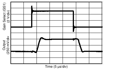
VDIFF = 20 mV VOUT at 25-V/V Gain = 500 mV
VOUT at 50-V/V Gain = 1 V
Figure 6-26 Gain Change Output Response (Gain = 25 V/V to 50 V/V)
GUID-027F5E8D-3423-4864-9068-451505D9DFF1-low.png
VDIFF = 20 mV VOUT at 50-V/V Gain = 1 V
VOUT at 200-V/V Gain = 4 V
Figure 6-28 Gain Change Output Response (Gain = 50 V/V to 200 V/V)
GUID-8CA14F78-62FB-47F5-94B9-21FF8810DF5F-low.png


Figure 6-30 Gain Change Output Response From Saturation (Gain = 50 V/V to 25 V/V)
GUID-0ABB2618-797F-41F7-ADAC-2118B691C51B-low.png


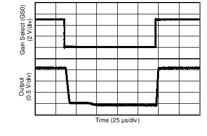
Figure 6-32 Gain Change Output Response From Saturation (Gain = 200 V/V to 50 V/V)
GUID-D63E106E-848B-4C6C-B21E-229B5AA0DA44-low.png


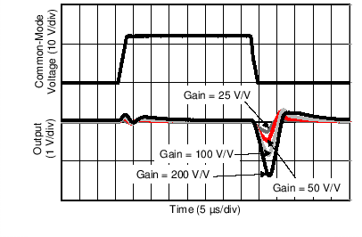
Figure 6-34 Common-Mode Voltage Transient Response