SBOS612A February 2014 – March 2014 INA225
PRODUCTION DATA.
- 1 Features
- 2 Applications
- 3 Description
- 4 Revision History
- 5 Terminal Configuration and Functions
- 6 Specifications
- 7 Detailed Description
- 8 Applications and Implementation
- 9 Power Supply Recommendations
- 10Layout
- 11Device and Documentation Support
- 12Mechanical, Packaging, and Orderable Information
Package Options
Mechanical Data (Package|Pins)
- DGK|8
Thermal pad, mechanical data (Package|Pins)
Orderable Information
6 Specifications
6.1 Absolute Maximum Ratings(1)
Over operating free-air temperature range, unless otherwise noted.| MIN | MAX | UNIT | ||
|---|---|---|---|---|
| Supply voltage | +40 | V | ||
| Analog inputs, VIN+, VIN–(2) | Differential (VIN+) – (VIN–) | –40 | +40 | V |
| Common-mode(3) | GND – 0.3 | +40 | V | |
| REF, GS0, and GS1 inputs | GND – 0.3 | (VS) + 0.3 | V | |
| Output | GND – 0.3 | (VS) + 0.3 | V | |
| Temperature | Operating, TA | –55 | +150 | °C |
| Junction, TJ | +150 | °C | ||
(1) Stresses beyond those listed under Absolute Maximum Ratings may cause permanent damage to the device. These are stress ratings only, which do not imply functional operation of the device at these or any other conditions beyond those indicated under Recommended Operating Conditions. Exposure to absolute-maximum-rated conditions for extended periods may affect device reliability.
(2) VIN+ and VIN– are the voltages at the IN+ and IN– terminals, respectively.
(3) Input voltage at any terminal may exceed the voltage shown if the current at that terminal is limited to 5 mA.
6.2 Handling Ratings
| MIN | MAX | UNIT | ||
|---|---|---|---|---|
| TSTG | Storage temperature range | –65 | +150 | °C |
| VESD(1) | Human body model (HBM) stress voltage(2) | 4 | kV | |
| Charged device model (CDM) stress voltage(3) | 1 | kV |
(1) Electrostatic discharge (ESD) to measure device sensitivity and immunity to damage caused by assembly line electrostatic discharges in to the device.
(2) Level listed above is the passing level per ANSI, ESDA, and JEDEC JS-001. JEDEC document JEP155 states that 4-kV HBM allows safe manufacturing with a standard ESD control process.
(3) Level listed above is the passing level per EIA-JEDEC JESD22-C101. JEDEC document JEP157 states that 1-kV CDM allows safe manufacturing with a standard ESD control process.
6.3 Recommended Operating Conditions
Over operating free-air temperature range, unless otherwise noted.| MIN | NOM | MAX | UNIT | ||
|---|---|---|---|---|---|
| VCM | Common-mode input voltage | 12 | V | ||
| VS | Operating supply voltage | 5 | V | ||
| TA | Operating free-air temperature | –40 | +125 | °C | |
6.4 Thermal Information
| THERMAL METRIC | INA225 | UNIT | |
|---|---|---|---|
| DGK (MSOP) | |||
| 8 TERMINALS | |||
| θJA | Junction-to-ambient thermal resistance | 163.6 | °C/W |
| θJCtop | Junction-to-case (top) thermal resistance | 57.7 | |
| θJB | Junction-to-board thermal resistance | 84.7 | |
| ψJT | Junction-to-top characterization parameter | 6.5 | |
| ψJB | Junction-to-board characterization parameter | 83.2 | |
| θJCbot | Junction-to-case (bottom) thermal resistance | N/A | |
6.5 Electrical Characteristics
At TA = +25°C, VSENSE = VIN+ – VIN–, VS = +5 V, VIN+ = 12 V, and VREF = VS / 2, unless otherwise noted.| PARAMETER | CONDITIONS | MIN | TYP | MAX | UNIT | ||
|---|---|---|---|---|---|---|---|
| INPUT | |||||||
| VCM | Common-mode input range | TA = –40°C to +125°C | 0 | 36 | V | ||
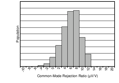
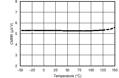
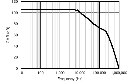
| CMR | Common-mode rejection | VIN+ = 0 V to +36 V, VSENSE = 0 mV, TA = –40°C to +125°C |
95 | 105 | dB | ||
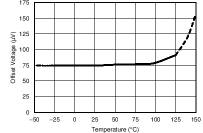
| VOS | Offset voltage, RTI(1) | VSENSE = 0 mV | ±75 | ±150 | μV | ||
| dVOS/dT | RTI vs temperature | TA = –40°C to +125°C | 0.2 | 0.5 | μV/°C | ||
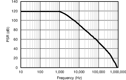
| PSRR | Power-supply rejection ratio | VSENSE = 0 mV, VREF = 2.5 V, VS = 2.7 V to 36 V |
±0.1 | ±1 | μV/V | ||
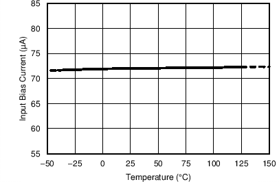
| IB | Input bias current | VSENSE = 0 mV | 55 | 72 | 85 | μA | |
| IOS | Input offset current | VSENSE = 0 mV | ±0.5 | μA | |||
| VREF | Reference input range | TA = –40°C to +125°C | 0 | VS | V | ||
| OUTPUT | |||||||
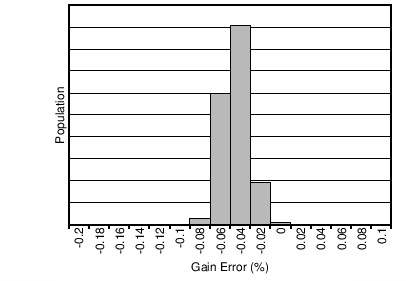
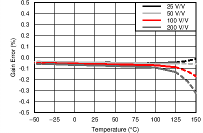
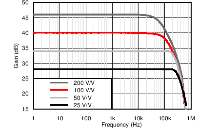
| G | Gain | 25, 50, 100, 200 | V/V | ||||
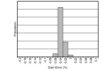
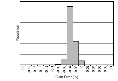
| EG | Gain error | Gain = 25 V/V and 50 V/V, VOUT = 0.5 V to VS – 0.5 V, TA = –40°C to +125°C |
±0.05% | ±0.15% | |||
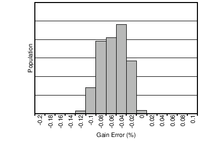
| Gain = 100 V/V, VOUT = 0.5 V to VS – 0.5 V, TA = –40°C to +125°C |
±0.1% | ±0.2% | |||||
| Gain = 200 V/V, VOUT = 0.5 V to VS – 0.5 V, TA = –40°C to +125°C |
±0.1% | ±0.3% | |||||
| Gain error vs temperature | G = 25 V/V, 50 V/V, 100 V/V, TA = –40°C to +125°C |
3 | 10 | ppm/°C | |||
| G = 200 V/V, TA = –40°C to +125°C | 5 | 15 | |||||
| Nonlinearity error | VOUT = 0.5 V to VS – 0.5 V | ±0.01% | |||||
| Maximum capacitive load | No sustained oscillation | 1 | nF | ||||
| VOLTAGE OUTPUT(2) | |||||||
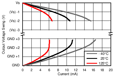
| Swing to VS power-supply rail | RL = 10 kΩ to GND, TA = –40°C to +125°C | VS – 0.05 | VS – 0.2 | V | |||
| Swing to GND(3) | VREF = VS / 2, all gains, RL = 10 kΩ to GND, TA = –40°C to +125°C |
VGND + 5 | VGND + 10 | mV | |||
| VREF = GND, gain = 25 V/V, RL = 10 kΩ to GND, TA = –40°C to +125°C |
VGND + 7 | mV | |||||
| VREF = GND, gain = 50 V/V, RL = 10 kΩ to GND, TA = –40°C to +125°C |
VGND + 15 | mV | |||||
| VREF = GND, gain = 100 V/V, RL = 10 kΩ to GND, TA = –40°C to +125°C |
VGND + 30 | mV | |||||
| VREF = GND, gain = 200 V/V, RL = 10 kΩ to GND, TA = –40°C to +125°C |
VGND + 60 | mV | |||||
| FREQUENCY RESPONSE | |||||||
| BW | Bandwidth | Gain = 25 V/V, CLOAD = 10 pF | 250 | kHz | |||
| Gain = 50 V/V, CLOAD = 10 pF | 200 | kHz | |||||
| Gain = 100 V/V, CLOAD = 10 pF | 125 | kHz | |||||
| Gain = 200 V/V, CLOAD = 10 pF | 70 | kHz | |||||
| SR | Slew rate | 0.4 | V/μs | ||||
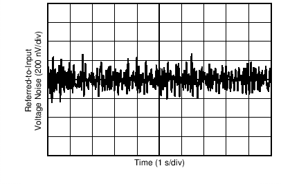
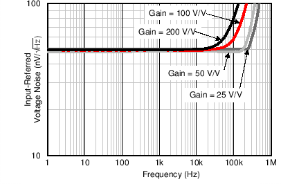
| NOISE, RTI(1) | |||||||
| Voltage noise density | 50 | nV/√Hz | |||||
| DIGITAL INPUT | |||||||
| Ci | Input capacitance | 3 | pF | ||||
| Leakage input current | 0 ≤ VIN ≤ VS | 1 | 2 | μA | |||
| VIL | Low-level input logic level | 0 | 0.6 | V | |||
| VIH | High-level input logic level | 2 | VS | V | |||
| POWER SUPPLY | |||||||
| VS | Operating voltage range | TA = –40°C to +125°C | +2.7 | +36 | V | ||
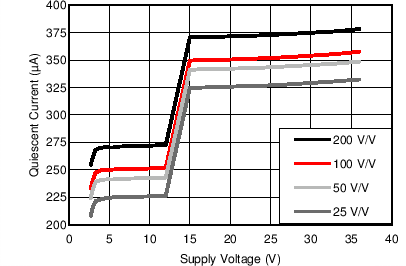
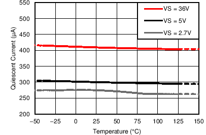
| IQ | Quiescent current | VSENSE = 0 mV | 300 | 350 | μA | ||
| IQ over temperature | TA = –40°C to +125°C | 375 | μA | ||||
| TEMPERATURE RANGE | |||||||
| Specified range | –40 | +125 | °C | ||||
| Operating range | –55 | +150 | °C | ||||
(1) RTI = referred-to-input.
(2) See Typical Characteristic curve, Output Voltage Swing vs Output Current (Figure 10).
(3) See Typical Characteristic curve, Unidirectional Output Voltage Swing vs. Temperature (Figure 14)
6.6 Typical Characteristics
At TA = +25°C, VS = +5 V, VIN+ = 12 V, and VREF = VS / 2, unless otherwise noted.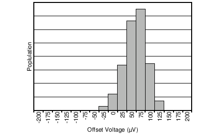
(Gain = 100 V/V)
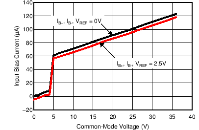
| VCM = 0 V | VREF = 2.5 V | VSENSE = 0 mV, Shorted | |
| VS = 5 V + 250-mV Sine Disturbance | |||
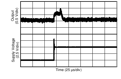
(Supply Voltage = +5 V)
| VS = 5 V | VCM = 12 V | |
| VS = ± 2.5 V | VCM = 0 V | VSENSE = 0 mV, Shorted | |
(Referred-to-Input)
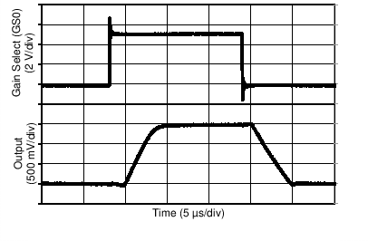
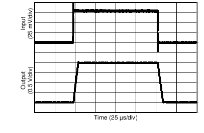
(Gain = 50 V/V, 2-VPP Output Step)
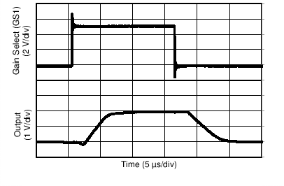
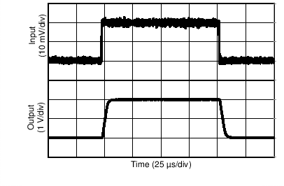
(Gain = 200 V/V, 2-VPP Output Step)
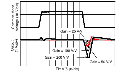
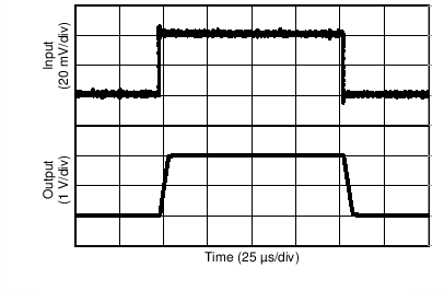
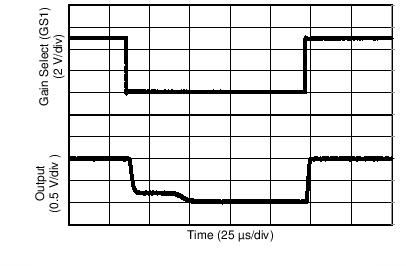
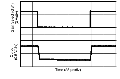
| VDIFF = 20 mV | VOUT at 25-V/V Gain = 500 mV | |
| VOUT at 100-V/V Gain = 2 V | ||
(Gain = 25 V/V to 100 V/V)
| VDIFF = 20 mV | VOUT at 100-V/V Gain = 2 V | |
| VOUT at 200-V/V Gain = 4 V | ||
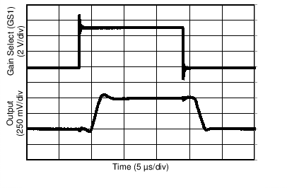
(Gain = 100 V/V to 200 V/V)

(Gain = 100 V/V to 25 V/V)
(Gain = 200 V/V to 100 V/V)
(Gain = 200 V/V)
| VCM = 0 V | VSENSE = 15 mVPP | |
| VS = 5 V | VREF = 2.5 V | VSENSE = 0 mV, Shorted | |
| VCM = 1-V Sine Wave | |||
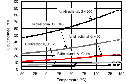
| Unidirectional, REF = GND | Bidirectional, REF > GND | ||
(Supply Voltage = 0 V, Shutdown)
| VS = ± 2.5 V | VREF = 0 V | VSENSE = 0 mV, Shorted | |
(Gain = 25 V/V, 2-VPP Output Step)
(Gain = 100 V/V, 2-VPP Output Step)
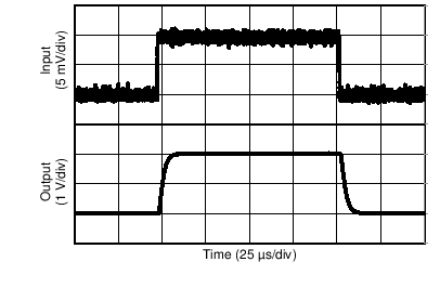
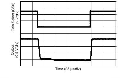
| VDIFF = 20 mV | VOUT at 25-V/V Gain = 500 mV | |
| VOUT at 50-V/V Gain = 1 V | ||
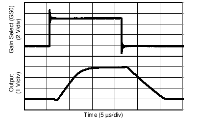
(Gain = 25 V/V to 50 V/V)
| VDIFF = 20 mV | VOUT at 50-V/V Gain = 1 V | |
| VOUT at 200-V/V Gain = 4 V | ||
(Gain = 50 V/V to 200 V/V)
(Gain = 50 V/V to 25 V/V)
(Gain = 200 V/V to 50 V/V)