SBOS381E February   2007  – January 2018 INA270 , INA271

PRODUCTION DATA.  

  1. Features
  2. Applications
  3. Description
    1.     Device Images
      1.      Simplified Schematic
  4. Revision History
  5. Device Comparison Table
  6. Pin Configuration and Functions
    1.     Pin Functions
  7. Specifications
    1. 7.1 Absolute Maximum Ratings
    2. 7.2 ESD Ratings
    3. 7.3 Recommended Operating Conditions
    4. 7.4 Thermal Information
    5. 7.5 Electrical Characteristics
    6. 7.6 Typical Characteristics
  8. Detailed Description
    1. 8.1 Overview
    2. 8.2 Functional Block Diagram
    3. 8.3 Feature Description
      1. 8.3.1 Basic Connection
      2. 8.3.2 Selecting RS
      3. 8.3.3 Transient Protection
    4. 8.4 Device Functional Modes
      1. 8.4.1 First- or Second-Order Filtering
      2. 8.4.2 Accuracy Variations as a Result of VSENSE and Common-Mode Voltage
        1. 8.4.2.1 Normal Case 1: VSENSE ≥ 20 mV, VCM ≥ VS
        2. 8.4.2.2 Normal Case 2: VSENSE ≥ 20 mV, VCM < VS
        3. 8.4.2.3 Low VSENSE Case 1: VSENSE < 20 mV, –16 V ≤ VCM < 0; and Low VSENSE Case 3: VSENSE < 20 mV, VS < VCM ≤ 80 V
        4. 8.4.2.4 Low VSENSE Case 2: VSENSE < 20 mV, 0 V ≤ VCM ≤ VS
  9. Application and Implementation
    1. 9.1 Application Information
    2. 9.2 Typical Application
      1. 9.2.1 Design Requirements
      2. 9.2.2 Detailed Design Procedure
      3. 9.2.3 Application Curves
  10. 10Power Supply Recommendations
    1. 10.1 Shutdown
  11. 11Layout
    1. 11.1 Layout Guidelines
      1. 11.1.1 RFI and EMI
    2. 11.2 Layout Example
  12. 12Device and Documentation Support
    1. 12.1 Documentation Support
      1. 12.1.1 Related Documentation
    2. 12.2 Related Links
    3. 12.3 Community Resources
    4. 12.4 Trademarks
    5. 12.5 Electrostatic Discharge Caution
    6. 12.6 Glossary
  13. 13Mechanical, Packaging, and Orderable Information

Package Options

Mechanical Data (Package|Pins)
Thermal pad, mechanical data (Package|Pins)
Orderable Information

Typical Characteristics

At TA = +25°C, VS = +12 V, VCM = 12 V, and VSENSE = 100 mV, unless otherwise noted.
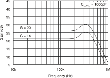
INA270 INA271 tc_g-frq_cl1k_bos381.gif
Figure 1. Gain vs Frequency
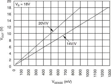
INA270 INA271 tc_gplot_bos381.gif
Figure 3. Gain Plot
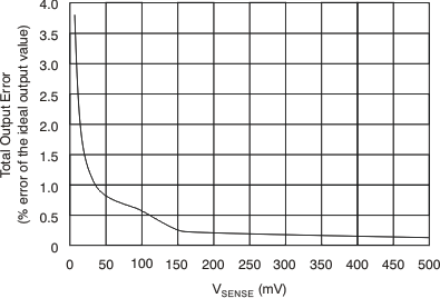
INA270 INA271 tc_err-vsense_bos381.gif
Figure 5. Total Output Error vs VSENSE
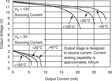
INA270 INA271 tc_pos_swing-io_bos381.gif
Figure 7. Positive Output Voltage Swing vs Output Current
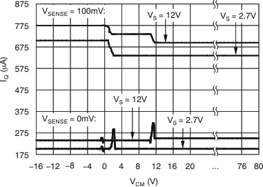
INA270 INA271 tc_iq-vcm_bos381.gif
Figure 9. Quiescent Current vs Common-Mode Voltage
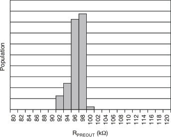
INA270 INA271 tc_histo_bos381.gif
Figure 11. PRE OUT Output Resistance Production Distribution
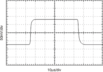
INA270 INA271 tc_step_sm_bos381.gif
Figure 13. Small-Signal Step Response
(10-mV to 20-mV Input)
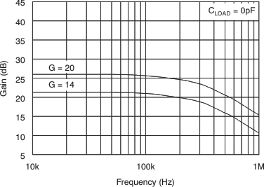
INA270 INA271 tc_g-frq_cl0_bos381.gif
Figure 2. Gain vs Frequency
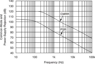
INA270 INA271 tc_cmrr_psrr-frq_bos381.gif
Figure 4. Common-Mode and Power-Supply Rejection vs Frequency
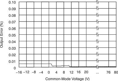
INA270 INA271 tc_err-vcm_bos381.gif
Figure 6. Output Error vs Common-Mode Voltage
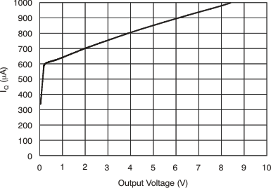
INA270 INA271 tc_iq-vo_bos381.gif
Figure 8. Quiescent Current vs Output Voltage
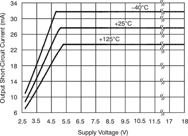
INA270 INA271 tc_cur-vs_bos381.gif
Figure 10. Output Short-Circuit Current vs Supply Voltage
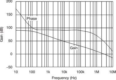
INA270 INA271 tc_buf_g-frq_bos381.gif
Figure 12. Buffer Gain vs Frequency
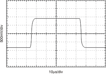
INA270 INA271 tc_step_lg_bos381.gif
Figure 14. Large-Signal Step Response
(10-mV to 100-mV Input)