SBOS870C May 2019 – August 2022 INA293-Q1
PRODUCTION DATA
- 1 Features
- 2 Applications
- 3 Description
- 4 Revision History
- 5 Pin Configuration and Functions
- 6 Specifications
- 7 Detailed Description
- 8 Application and Implementation
- 9 Device and Documentation Support
- 10Mechanical, Packaging, and Orderable Information
Package Options
Mechanical Data (Package|Pins)
- DBV|5
Thermal pad, mechanical data (Package|Pins)
Orderable Information
8.1.1 RSENSE and Device Gain Selection
The accuracy of any current-sense amplifier is maximized by choosing the current-sense resistor to be as large as possible. A large sense resistor maximizes the differential input signal for a given amount of current flow and reduces the error contribution of the offset voltage. However, there are practical limits as to how large the current-sense resistor can be in a given application because of the resistor size and maximum allowable power dissipation. Equation 1 gives the maximum value for the current-sense resistor for a given power dissipation budget:
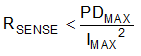
where:
- PDMAX is the maximum allowable power dissipation in RSENSE.
- IMAX is the maximum current that will flow through RSENSE.
An additional limitation on the size of the current-sense resistor and device gain is due to the power-supply voltage, VS, and device swing-to-rail limitations. To make sure that the current-sense signal is properly passed to the output, both positive and negative output swing limitations must be examined. Equation 2 provides the maximum values of RSENSE and GAIN to keep the device from exceeding the positive swing limitation.
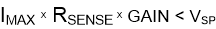
where:
- IMAX is the maximum current that will flow through RSENSE.
- GAIN is the gain of the current-sense amplifier.
- VSP is the positive output swing as specified in the data sheet.
To avoid positive output swing limitations when selecting the value of RSENSE, there is always a trade-off between the value of the sense resistor and the gain of the device under consideration. If the sense resistor selected for the maximum power dissipation is too large, then it is possible to select a lower-gain device in order to avoid positive swing limitations.
The negative swing limitation places a limit on how small the sense resistor value can be for a given application. Equation 3 provides the limit on the minimum value of the sense resistor.
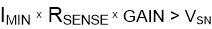
where:
- IMIN is the minimum current that will flow through RSENSE.
- GAIN is the gain of the current-sense amplifier.
- VSN is the negative output swing of the device.
Table 8-1 shows an example of the different results obtained from using five different gain versions of the INA293-Q1. From the table data, the highest gain device allows a smaller current-shunt resistor and decreased power dissipation in the element.
| PARAMETER | EQUATION | RESULTS AT VS = 5 V | |||||
|---|---|---|---|---|---|---|---|
| A1, B1 DEVICES | A2, B2 DEVICES | A3, B3 DEVICES | A4, B4 DEVICES | A5, B5 DEVICES | |||
| G | Gain | 20 V/V | 50 V/V | 100 V/V | 200 V/V | 500 V/V | |
| VDIFF | Ideal differential input voltage | VDIFF = VOUT / G | 250 mV | 100 mV | 50 mV | 25 mV | 10 mV |
| RSENSE | Current sense resistor value | RSENSE = VDIFF / IMAX | 25 mΩ | 10 mΩ | 5 mΩ | 2.5 mΩ | 1 mΩ |
| PSENSE | Current-sense resistor power dissipation | RSENSE × IMAX2 | 2.5 W | 1 W | 0.5W | 0.25 W | 0.1 W |