SBOS713A September 2015 – February 2016 INA301
PRODUCTION DATA.
- 1 Features
- 2 Applications
- 3 Description
- 4 Revision History
- 5 Pin Configuration and Functions
- 6 Specifications
- 7 Detailed Description
- 8 Applications and Implementation
- 9 Power Supply Recommendations
- 10Layout
- 11Device and Documentation Support
- 12Mechanical, Packaging, and Orderable Information
Package Options
Mechanical Data (Package|Pins)
- DGK|8
Thermal pad, mechanical data (Package|Pins)
Orderable Information
10 Layout
10.1 Layout Guidelines
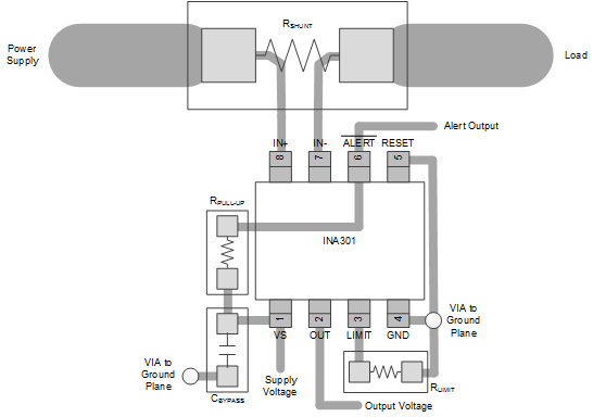
- Place the power-supply bypass capacitor as closely as possible to the supply and ground pins. The recommended value of this bypass capacitor is 0.1 µF. Additional decoupling capacitance can be added to compensate for noisy or high-impedance power supplies.
- Make the connection of RLIMIT to the ground pin as direct as possible to limit additional capacitance on this node. Routing this connection must be limited to the same plane if possible to avoid vias to internal planes. If the routing can not be made on the same plane and must pass through vias, ensure that a path is routed from RLIMIT back to the ground pin and that RLIMIT is not simply connected directly to a ground plane.
- The open-drain output pin is recommended to be pulled up to the supply voltage rail through a 10-kΩ pullup resistor.
10.2 Layout Example

NOTE:
Connect the limit resistor directly to the GND pin.