SBOS896 November 2017 INA317
PRODUCTION DATA.
- 1 Features
- 2 Applications
- 3 Description
- 4 Revision History
- 5 Pin Configuration and Functions
- 6 Specifications
- 7 Detailed Description
- 8 Application and Implementation
- 9 Power Supply Recommendations
- 10Layout
- 11Device and Documentation Support
- 12Mechanical, Packaging, and Orderable Information
Package Options
Mechanical Data (Package|Pins)
- DGK|8
Thermal pad, mechanical data (Package|Pins)
Orderable Information
7 Detailed Description
7.1 Overview
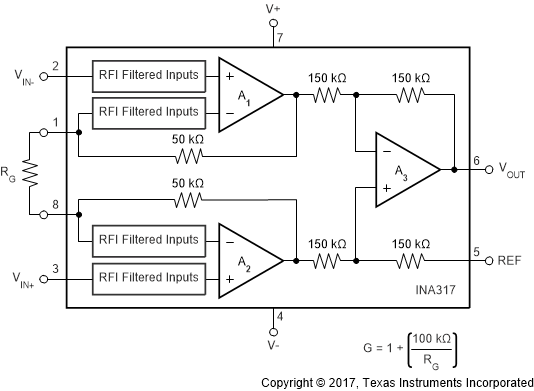
The INA317 is a monolithic instrumentation amplifier (INA) based on the precision zero-drift OPA333 (operational amplifier) core. The INA317 integrates laser-trimmed resistors to ensure excellent common-mode rejection and low gain error. The combination of the zero-drift amplifier core and the precision resistors allows this device to achieve outstanding DC precision and is designed for 3.3-V and 5-V industrial applications.
7.2 Functional Block Diagram

7.3 Feature Description
The INA317 is a low-power, zero-drift instrumentation amplifier that offers accuracy. The versatile three-operational-amplifier design and small size makes the amplifier designed for a wide range of applications. Zero-drift chopper circuitry provides DC specifications. A single external resistor sets any gain from 1 to 10,000. The INA317 is laser trimmed for high common-mode rejection (100 dB at G ≥ 100). Typically, the INA317 operates with power supplies as low as 1.8 V and quiescent current of 50 µA.
7.4 Device Functional Modes
7.4.1 Internal Offset Correction
INA317 internal operational amplifiers use an autocalibration technique with a time-continuous 350-kHz operational amplifier in the signal path. The amplifier is zero-corrected every 8 µs using a proprietary technique. Upon power up, the amplifier requires approximately 100 µs to achieve specified VOS accuracy. This design has no aliasing or flicker noise.
7.4.2 Input Common-Mode Range
The linear input voltage range of the input circuitry of the INA317 is from approximately 0.1 V below the positive supply voltage to 0.1 V above the negative supply. However, as a differential input voltage causes the output voltage to increase, the output voltage swing of amplifiers A1 and A2 limits the linear input range. As a result, the linear common-mode input range is related to the output voltage of the complete amplifier. This behavior depends on supply voltage; see Figure 20.
Input overload conditions can produce an output voltage that appears normal. For example, if an input overload condition drives the input amplifiers to the respective positive output swing limit, the difference voltage measured by the output amplifier is approximately zero. The output of the INA317 is approximately 0 V even though the inputs are overloaded.