SLLSE83F April 2013 – January 2015 ISO7131CC , ISO7140CC , ISO7140FCC , ISO7141CC , ISO7141FCC
PRODUCTION DATA.
- 1 Features
- 2 Applications
- 3 Description
- 4 Revision History
- 5 Pin Configuration and Functions
-
6 Specifications
- 6.1 Absolute Maximum Ratings
- 6.2 ESD Ratings
- 6.3 Recommended Operating Conditions
- 6.4 Thermal Information
- 6.5 Power Dissipation Ratings
- 6.6 Electrical Characteristics: VCC1 and VCC2 at 5 V ±10%
- 6.7 Electrical Characteristics: VCC1 and VCC2 at 3.3 V ±10%
- 6.8 Electrical Characteristics: VCC1 and VCC2 at 2.7 V
- 6.9 Switching Characteristics: VCC1 and VCC2 at 5 V ±10%
- 6.10 Switching Characteristics: VCC1 and VCC2 at 3.3 V ±10%
- 6.11 Switching Characteristics: VCC1 and VCC2 at 2.7 V
- 6.12 Supply Current: VCC1 and VCC2 at 5 V ±10%
- 6.13 Supply Current: VCC1 and VCC2 at 3.3 V ±10%
- 6.14 Supply Current: VCC1 and VCC2 at 2.7 V
- 6.15 Typical Characteristics
- 7 Parameter Measurement Information
- 8 Detailed Description
- 9 Application and Implementation
- 10Power Supply Recommendations
- 11Layout
- 12Device and Documentation Support
- 13Mechanical, Packaging, and Orderable Information
Package Options
Mechanical Data (Package|Pins)
- DBQ|16
Thermal pad, mechanical data (Package|Pins)
Orderable Information
7 Parameter Measurement Information
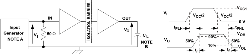
A. The input pulse is supplied by a generator having the following characteristics: PRR ≤ 50 kHz, 50% duty cycle, tr ≤ 3 ns, tf ≤ 3 ns, ZO = 50 Ω. At the input, a 50-Ω resistor is required to terminate the input-generator signal. It is not needed in an actual application.
B. CL = 15 pF and includes instrumentation and fixture capacitance within ±20%.
Figure 10. Switching-Characteristics Test Circuit and Voltage Waveforms
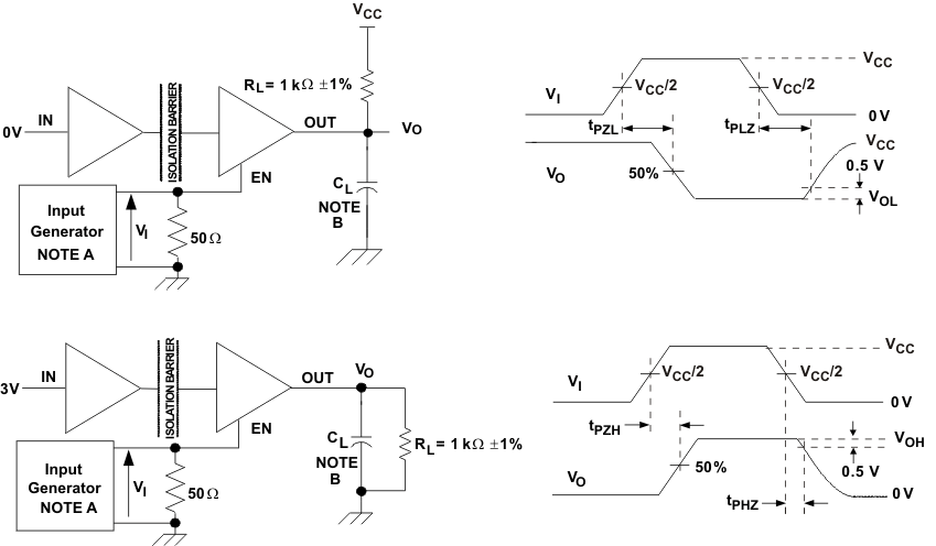
A. The input pulse is supplied by a generator having the following characteristics: PRR ≤ 50 kHz, 50% duty cycle, tr ≤ 3 ns, tf ≤ 3 ns, ZO = 50 Ω.
B. CL = 15 pF and includes instrumentation and fixture capacitance within ±20%.
Figure 11. Enable/Disable Propagation Delay-Time Test Circuit and Waveform
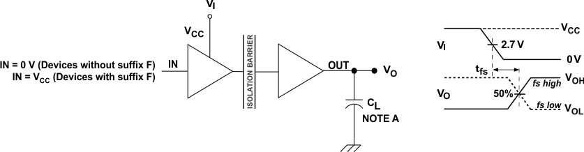
A. CL = 15 pF and includes instrumentation and fixture capacitance within ±20%.
Figure 12. Failsafe Delay-Time Test Circuit and Voltage Waveforms
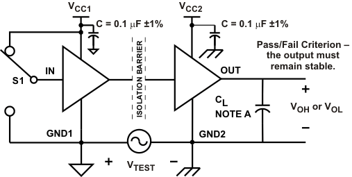
A. CL = 15 pF and includes instrumentation and fixture capacitance within ±20%.
Figure 13. Common-Mode Transient Immunity Test Circuit