SLLSE39E June   2010  – May 2015 ISO7520C , ISO7521C

PRODUCTION DATA.  

  1. Features
  2. Applications
  3. Description
  4. Revision History
  5. Pin Configuration and Functions
  6. Specifications
    1. 6.1  Absolute Maximum Ratings
    2. 6.2  ESD Ratings
    3. 6.3  Recommended Operating Conditions
    4. 6.4  Thermal Information
    5. 6.5  Electrical Characteristics: VCC1 and VCC2 at 5 V ± 5%
    6. 6.6  Electrical Characteristics: VCC1 at 5 V ± 5%, VCC2 at 3.3 V ± 5%
    7. 6.7  Electrical Characteristics: VCC1 at 3.3 V ± 5%, VCC2 at 5 V ± 5%
    8. 6.8  Electrical Characteristics: VCC1 and VCC2 at 3.3 V ± 5%
    9. 6.9  Switching Characteristics: VCC1 and VCC2 at 5 V ± 5%
    10. 6.10 Switching Characteristics: VCC1 at 5 V ± 5%, VCC2 at 3.3 V ± 5%
    11. 6.11 Switching Characteristics: VCC1 at 3.3 V ± 5%, VCC2 at 5 V ± 5%
    12. 6.12 Switching Characteristics: VCC1 and VCC2 at 3.3 V ± 5%
    13. 6.13 Typical Characteristics
  7. Parameter Measurement Information
  8. Detailed Description
    1. 8.1 Overview
    2. 8.2 Functional Block Diagram
    3. 8.3 Feature Description
      1. 8.3.1 Insulation Characteristics
      2. 8.3.2 IEC 60664-1 Ratings Table
      3. 8.3.3 Package Insulation and Safety-Related Specifications
      4. 8.3.4 Safety Limiting Values
      5. 8.3.5 Regulatory Information
    4. 8.4 Device Functional Modes
  9. Application and Implementation
    1. 9.1 Application Information
    2. 9.2 Typical Application
      1. 9.2.1 Design Requirements
      2. 9.2.2 Detailed Design Procedure
      3. 9.2.3 Application Curve
  10. 10Power Supply Recommendations
  11. 11Layout
    1. 11.1 Layout Guidelines
      1. 11.1.1 PCB Material
    2. 11.2 Layout Example
  12. 12Device and Documentation Support
    1. 12.1 Documentation Support
      1. 12.1.1 Related Documentation
    2. 12.2 Related Links
    3. 12.3 Community Resources
    4. 12.4 Trademarks
    5. 12.5 Electrostatic Discharge Caution
    6. 12.6 Glossary
  13. 13Mechanical, Packaging, and Orderable Information

Package Options

Mechanical Data (Package|Pins)
Thermal pad, mechanical data (Package|Pins)
Orderable Information

5 Pin Configuration and Functions

DW Package
16-Pin SOIC
Top View
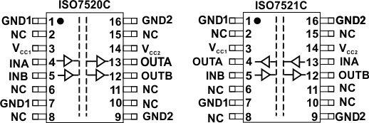
ISO7520C ISO7521C POs2_llse39.gif

Pin Functions

PIN I/O DESCRIPTION
NAME ISO7520C ISO7521C
GND1 1, 7 1, 7 Ground connection for VCC1
GND2 9, 16 9, 16 Ground connection for VCC2
INA 4 13 I Input, channel A
INB 5 5 I Input, channel B
NC 2, 6, 8, 10, 11, 15 2, 6, 8, 10, 11, 15 No internal connection
OUTA 13 4 O Output, channel A
OUTB 12 12 O Output, channel B
VCC1 3 3 Power supply, VCC1
VCC2 14 14 Power supply, VCC2