SLLSEC3F September 2012 – April 2016 ISO7631FC , ISO7631FM , ISO7641FC
PRODUCTION DATA.
- 1 Features
- 2 Applications
- 3 Description
- 4 Revision History
- 5 Pin Configuration and Functions
-
6 Specifications
- 6.1 Absolute Maximum Ratings
- 6.2 ESD Ratings
- 6.3 Recommended Operating Conditions
- 6.4 Thermal Information
- 6.5 Electrical Characteristics: VCC1 and VCC2 at 5 V ± 10%
- 6.6 Electrical Characteristics: VCC1 at 5 V ± 10% and VCC2 at 3.3 V ± 10%
- 6.7 Electrical Characteristics: VCC1 at 3.3 V ± 10% and VCC2 at 5 V ± 10%
- 6.8 Electrical Characteristics: VCC1 and VCC2 at 3.3 V ± 10%
- 6.9 Electrical Characteristics: VCC1 and VCC2 at 2.7 V (ISO7631FM Only)
- 6.10 Power Dissipation Characteristics
- 6.11 Supply Current Characteristics: VCC1 and VCC2 at 5 V ± 10%
- 6.12 Supply Current Characteristics: VCC1 at 5 V ± 10% and VCC2 at 3.3 V ± 10%
- 6.13 Supply Current Characteristics: VCC1 at 3.3 V ± 10% and VCC2 at 5 V ± 10%
- 6.14 Supply Current Characteristics: VCC1 and VCC2 at 3.3 V ± 10%
- 6.15 Supply Current Characteristics: VCC1 and VCC2 at 2.7 V (ISO7631FM Only) Only M-Grade devices are recommended for operation down to 2.7 V supplies. For 2.7 V-operation, max data rate is 100 Mbps.
- 6.16 Switching Characteristics: VCC1 and VCC2 at 5 V ± 10%
- 6.17 Switching Characteristics: VCC1 at 5 V ± 10% and VCC2 at 3.3 V ± 10%
- 6.18 Switching Characteristics: VCC1 at 3.3 V ± 10% and VCC2 at 5 V ± 10%
- 6.19 Switching Characteristics: VCC1 and VCC2 at 3.3 V ± 10%
- 6.20 Switching Characteristics: VCC1 and VCC2 at 2.7 V Only M-Grade devices are recommended for operation down to 2.7 V supplies. For 2.7 V-operation, max data rate is 100 Mbps.
- 6.21 Typical Characteristics
- 7 Parameter Measurement Information
- 8 Detailed Description
- 9 Application and Implementation
- 10Power Supply Recommendations
- 11Layout
- 12Device and Documentation Support
- 13Mechanical, Packaging, and Orderable Information
Package Options
Refer to the PDF data sheet for device specific package drawings
Mechanical Data (Package|Pins)
- DW|16
Thermal pad, mechanical data (Package|Pins)
Orderable Information
1 Features
- Signaling Rate: 150 Mbps (M-Grade), 25 Mbps (C-Grade)
- Robust Design with Integrated Noise Filter
(C-Grade) - Low Power Consumption, Typical ICC per Channel (3.3-V Supplies):
- Extremely-Low ICC_disable (C-Grade)
- Low Propagation Delay: 7 ns Typical (M-Grade)
- Output Defaults to Low-State in Fail-Safe Mode
- Wide Temperature Range: –40°C to 125°C
- 50 KV/µs Transient Immunity, Typical
- Long Life With SiO2 Isolation Barrier
- Operates From 2.7-V (M-Grade), 3.3-V and 5-V Supply and Logic Levels
- 2.7-V (M-Grade), 3.3-V and 5-V Level Translation
- Wide Body SOIC-16 Package
- Safety and Regulatory Approvals
- 2500 VRMS Isolation for 1 Minute per UL 1577
- 4242 VPK Basic Insulation per DIN V VDE V 0884-10 and DIN EN 61010-1
- CSA Component Acceptance Notice 5A, IEC 60950-1 and IEC 61010-1 End Equipment Standards
- CQC Certification per GB4943.1-2011
- TUV 3000 VRMS Reinforced Insulation according to EN/UL/CSA 60950-1 and EN/UL/CSA 61010-1
2 Applications
- Optocoupler Replacement in:
- Industrial Fieldbus
- Profibus
- Modbus
- DeviceNet™ Data Buses
- Servo Control Interface
- Motor Control
- Power Supplies
- Battery Packs
- Industrial Fieldbus
3 Description
The ISO7631F and ISO7641F devices provide galvanic isolation up to 4242 VPK per VDE. The ISO7631F device has three channels, two of which operate in the forward direction and one which operates in the reverse direction. The ISO7641F device has 4 channels, three of which operate in the forward direction and one of which operates in the reverse direction. Suffix F indicates that output defaults to low-state in fail-safe conditions (see ). M-Grade devices are high-speed isolators capable of up to150-Mbps data rates with fast propagation delays, whereas C-Grade devices are capable of up to 25-Mbps data rates with low power consumption and integrated filters for noise-prone applications. C-Grade devices are recommended for lower-speed applications where input noise pulses of less than 6 ns duration must be suppressed, or when low-power consumption is critical.
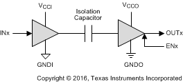
Each isolation channel has a logic input and output buffer separated by a silicon dioxide (SiO2) insulation barrier. Used in conjunction with isolated power supplies, these devices prevent noise currents on a data bus or other circuits from entering the local ground and interfering with or damaging sensitive circuitry. The devices have TTL input thresholds and can operate from 2.7-V (M-Grade), 3.3-V and 5-V supplies. All inputs are 5-V tolerant when supplied from 3.3-V or 2.7-V supplies.
Device Information(1)
| PART NUMBER | PACKAGE | BODY SIZE (NOM) |
|---|---|---|
| ISO7631FM | SOIC (16) | 10.30 mm × 7.50 mm |
| ISO7631FC | ||
| ISO7641FC |
- For all available packages, see the orderable addendum at the end of the datasheet.
Simplified Schematic
