SLLSET8A March 2016 – August 2016 ISO7820LL , ISO7821LL
PRODUCTION DATA.
- 1 Features
- 2 Applications
- 3 Description
- 4 Revision History
- 5 Pin Configuration and Functions
-
6 Specifications
- 6.1 Absolute Maximum Ratings
- 6.2 ESD Ratings
- 6.3 Recommended Operating Conditions
- 6.4 Thermal Information
- 6.5 Power Ratings
- 6.6 Insulation Specifications
- 6.7 Safety-Related Certifications
- 6.8 Safety Limiting Values
- 6.9 DC Electrical Characteristics
- 6.10 DC Supply Current Characteristics
- 6.11 Switching Characteristics
- 6.12 Insulation Characteristics Curves
- 6.13 Typical Characteristics
- 7 Parameter Measurement Information
- 8 Detailed Description
- 9 Application and Implementation
- 10Power Supply Recommendations
- 11Layout
- 12Device and Documentation Support
- 13Mechanical, Packaging, and Orderable Information
Package Options
Mechanical Data (Package|Pins)
Thermal pad, mechanical data (Package|Pins)
- DW|16
Orderable Information
11 Layout
11.1 Layout Guidelines
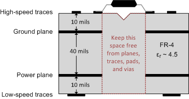
A minimum of four layers is required to accomplish a low EMI PCB design (see Figure 34). Layer stacking should be in the following order (top-to-bottom): high-speed signal layer, ground plane, power plane and low-frequency signal layer.
- Routing the high-speed traces on the top layer avoids the use of vias (and the introduction of their inductances) and allows for clean interconnects between the isolator and the transmitter and receiver circuits of the data link.
- Placing a solid ground plane next to the high-speed signal layer establishes controlled impedance for transmission line interconnects and provides an excellent low-inductance path for the return current flow.
- Placing the power plane next to the ground plane creates additional high-frequency bypass capacitance of approximately 100 pF/in2.
- Routing the slower speed control signals on the bottom layer allows for greater flexibility as these signal links usually have margin to tolerate discontinuities such as vias.
- While routing differential traces on a board, TI recommends that the distance between two differential pairs be much higher (at least 2x) than the distance between the traces in a differential pair. This distance minimizes crosstalk between the two differential pairs.
If an additional supply voltage plane or signal layer is needed, add a second power or ground plane system to the stack to keep it symmetrical. This makes the stack mechanically stable and prevents it from warping. Also the power and ground plane of each power system can be placed closer together, thus increasing the high-frequency bypass capacitance significantly.
The ISO782xLL family of devices requires no special layout considerations to mitigate electromagnetic
emissions.
For detailed layout recommendations, see the Digital Isolator Design Guide (SLLA284).
11.1.1 PCB Material
For digital circuit boards operating at less than 150 Mbps (or rise and fall times higher than 1 ns) and trace lengths of up to 10 inches, use standard FR–4 UL94V-0 epoxy-glass as PCB material. ThisPCB is preferred over cheaper alternatives because of lower dielectric losses at high frequencies, less moisture absorption, greater strength and stiffness, and self-extinguishing flammability-characteristics.
11.2 Layout Example
 Figure 34. Layout Example