SLLSET5A March 2016 – September 2016 ISO7821LLS
PRODUCTION DATA.
- 1 Features
- 2 Applications
- 3 Description
- 4 Revision History
- 5 Pin Configuration and Functions
-
6 Specifications
- 6.1 Absolute Maximum Ratings
- 6.2 ESD Ratings
- 6.3 Recommended Operating Conditions
- 6.4 Thermal Information
- 6.5 Power Ratings
- 6.6 Insulation Specifications
- 6.7 Safety-Related Certifications
- 6.8 Safety Limiting Values
- 6.9 DC Electrical Characteristics
- 6.10 DC Supply Current Characteristics
- 6.11 Timing Requirements for Distortion Correction Scheme
- 6.12 Switching Characteristics
- 6.13 Insulation Characteristics Curves
- 6.14 Typical Characteristics
- 7 Parameter Measurement Information
- 8 Detailed Description
- 9 Application and Implementation
- 10Power Supply Recommendations
- 11Layout
- 12Device and Documentation Support
- 13Mechanical, Packaging, and Orderable Information
Package Options
Mechanical Data (Package|Pins)
Thermal pad, mechanical data (Package|Pins)
- DW|16
Orderable Information
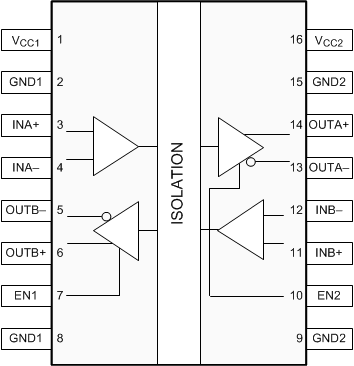
5 Pin Configuration and Functions
DW and DWW Packages
16-Pin SOIC
Top View

Pin Functions
| PIN | I/O | DESCRIPTION | |
|---|---|---|---|
| NAME | NO. | ||
| EN1 | 7 | I | Output enable 1. Output pins on side 1 are enabled when EN1 is high or open and in high impedance state when EN1 is low. |
| EN2 | 10 | I | Output enable 2. Output pins on side 2 are enabled when EN2 is high or open and in high impedance state when EN2 is low. |
| GND1 | 2 | — | Ground connection for VCC1 |
| 8 | |||
| GND2 | 9 | — | Ground connection for VCC2 |
| 15 | |||
| INA+ | 3 | I | Positive differential input, channel A |
| INA– | 4 | I | Negative differential input, channel A |
| INB+ | 11 | I | Positive differential input, channel B |
| INB– | 12 | I | Negative differential input, channel B |
| OUTA+ | 14 | O | Positive differential output, channel A |
| OUTA– | 13 | O | Negative differential output, channel A |
| OUTB+ | 6 | O | Positive differential output, channel B |
| OUTB– | 5 | O | Negative differential output, channel B |
| VCC1 | 1 | — | Power supply, side 1, VCC1 |
| VCC2 | 16 | — | Power supply, side 2, VCC2 |