SNOSCY1 March 2014 LDC1041
PRODUCTION DATA.
- 1 Features
- 2 Applications
- 3 Description
- 4 Revision History
- 5 Terminal Configuration and Functions
- 6 Specifications
- 7 Detailed Description
- 8 Applications and Implementation
- 9 Power Supply Recommendations
- 10Layout
- 11Device and Documentation Support
- 12Mechanical, Packaging, and Orderable Information
Package Options
Mechanical Data (Package|Pins)
- NHR|16
Thermal pad, mechanical data (Package|Pins)
Orderable Information
5 Terminal Configuration and Functions
WSON-16
Top View
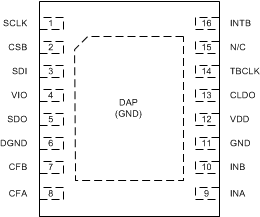
Terminal Description
| TERMINAL NAME | TERMINAL NO. |
TERMINAL TYPE (1) |
FUNCTION |
|---|---|---|---|
| SCLK | 1 | DO | SPI clock input. SCLK is used to clock-out/clock-in the data from/into the chip |
| CSB | 2 | DI | SPI CSB(Chip Select Bar). Multiple devices can be connected on the same SPI bus and CSB can be used to select the device to be communicated with |
| SDI | 3 | DI | SPI Slave Data In (Master Out Slave In). This should be connected to the Master Out Slave In of the master |
| VIO | 4 | P | Digital IO Supply |
| SDO | 5 | DO | SPI Slave Data Out (Master In Slave Out).It is high impedance when CSB is high |
| DGND | 6 | P | Digital ground |
| CFB | 7 | A | LDC filter capacitor |
| CFA | 8 | A | LDC filter capacitor |
| INA | 9 | A | External LC Tank. Connect to external LC tank |
| INB | 10 | A | External LC Tank. Connect to external LC tank |
| GND | 11 | P | Analog ground |
| VDD | 12 | P | Analog supply |
| CLDO | 13 | A | LDO bypass capacitor. A 56nF capacitor should be connected from this Terminal to GND |
| TBCLK | 14 | DI | External time-base clock |
| N/C | 15 | N/C | No Connection |
| INTB | 16 | DO | Configurable interrupt. This Terminal can be configured to behave in 3 different ways by programing the INT Terminal mode register. Either threshold detect, wakeup, or DRDYB |
| DAP | 17 | P | Connect to GND |
(1) DO: Digital Output, DI: Digital Input, P: Power, A: Analog