SNOSD01D May 2015 – October 2016 LDC1101
PRODUCTION DATA.
- 1 Features
- 2 Applications
- 3 Description
- 4 Simplified Schematic
- 5 Revision History
- 6 Pin Configuration and Functions
- 7 Specifications
-
8 Detailed Description
- 8.1 Overview
- 8.2 Functional Block Diagram
- 8.3 Feature Description
- 8.4
Device Functional Modes
- 8.4.1 Measurement Modes
- 8.4.2 RP+L Measurement Mode
- 8.4.3 High Resolution L (LHR) Measurement Mode
- 8.4.4 Reference Count Setting
- 8.4.5 L-Only Measurement Operation
- 8.4.6 Minimum Sensor Frequency and Watchdog Setting
- 8.4.7 Low Power Modes
- 8.4.8 Status Reporting
- 8.4.9 Switch Functionality and INTB Reporting
- 8.5 Programming
- 8.6
Register Maps
- 8.6.1 Individual Register Listings
- 8.6.2 Register RP_SET (address = 0x01) [reset = 0x07]
- 8.6.3 Register TC1 (address = 0x02) [reset = 0x90]
- 8.6.4 Register TC2 (address = 0x03) [reset = 0xA0]
- 8.6.5 Register DIG_CONF (address = 0x04) [reset = 0x03]
- 8.6.6 Register ALT_CONFIG (address = 0x05) [reset = 0x00]
- 8.6.7 Register RP_THRESH_HI_LSB (address = 0x06) [reset = 0x00]
- 8.6.8 Register RP_THRESH_HI_MSB (address = 0x07) [reset = 0x00]
- 8.6.9 Register RP_THRESH_LO_LSB (address = 0x08) [reset = 0x00]
- 8.6.10 Register RP_THRESH_LO_MSB (address = 0x09) [reset = 0x00]
- 8.6.11 Register INTB_MODE (address = 0x0A) [reset = 0x00]
- 8.6.12 9.Register START_CONFIG (address = 0x0B) [reset = 0x01]
- 8.6.13 Register D_CONFIG (address = 0x0C) [reset = 0x00]
- 8.6.14 Register L_THRESH_HI_LSB (address = 0x16) [reset = 0x00]
- 8.6.15 Register L_THRESH_HI_MSB (address = 0x17) [reset = 0x00]
- 8.6.16 Register L_THRESH_LO_LSB (address = 0x18) [reset = 0x00]
- 8.6.17 Register L_THRESH_LO_MSB (address = 0x19) [reset = 0x00]
- 8.6.18 Register STATUS (address = 0x020 [reset = 0x00]
- 8.6.19 Register RP_DATA_LSB (address = 0x21) [reset = 0x00]
- 8.6.20 Register RP_DATA_MSB (address = 0x22) [reset = 0x00]
- 8.6.21 Register L_DATA_LSB (address = 0x23) [reset = 0x00]
- 8.6.22 Register L_DATA_MSB (address = 0x24) [reset = 0x00]
- 8.6.23 Register LHR_RCOUNT_LSB (address = 0x30) [reset = 0x00]
- 8.6.24 Register LHR_RCOUNT_MSB (address = 0x31) [reset = 0x00]
- 8.6.25 Register LHR_OFFSET_LSB (address = 0x32) [reset = 0x00]
- 8.6.26 Register LHR_OFFSET_MSB (address = 0x33) [reset = 0x00]
- 8.6.27 Register LHR_CONFIG (address = 0x34) [reset = 0x00]
- 8.6.28 Register LHR_DATA_LSB (address = 0x38) [reset = 0x00]
- 8.6.29 Register LHR_DATA_MID (address = 0x39) [reset = 0x00]
- 8.6.30 Register LHR_DATA_MSB (address = 0x3A) [reset = 0x00]
- 8.6.31 Register LHR_STATUS (address = 0x3B) [reset = 0x00]
- 8.6.32 Register RID (address = 0x3E) [reset = 0x02]
- 8.6.33 Register DEVICE_ID (address = 0x3F) [reset = 0xD4]
-
9 Application and Implementation
- 9.1
Application Information
- 9.1.1 TI Designs and Application Notes
- 9.1.2 Theory of Operation
- 9.1.3 RP+L Mode Calculations
- 9.1.4 LDC1101 RP Configuration
- 9.1.5 Setting Internal Time Constant 1
- 9.1.6 Setting Internal Time Constant 2
- 9.1.7 MIN_FREQ and Watchdog Configuration
- 9.1.8 RP+L Sample Rate Configuration With RESP_TIME
- 9.1.9 High Resolution Inductance Calculation (LHR mode)
- 9.1.10 LHR Sample Rate Configuration With RCOUNT
- 9.1.11 Setting RPMIN for LHR Measurements
- 9.1.12 Sensor Input Divider
- 9.1.13 Reference Clock Input
- 9.1.14 INTB Reporting on SDO
- 9.1.15 DRDY (Data Ready) Reporting on SDO
- 9.1.16 Comparator Functionality
- 9.2 Typical Application
- 9.1
Application Information
- 10Power Supply Recommendations
- 11Layout
- 12Device and Documentation Support
- 13Mechanical, Packaging, and Orderable Information
Package Options
Mechanical Data (Package|Pins)
- DRC|10
Thermal pad, mechanical data (Package|Pins)
- DRC|10
Orderable Information
11 Layout
11.1 Layout Guidelines
The LDC1101 requires minimal external components for effective operation. Following good layout techniques providing good grounding and clean supplies are critical for optimum operation. Due to the small physical size of the LDC1101, use of surface mount 0402 or smaller components can ease routing.
11.1.1 Ground and Power Planes
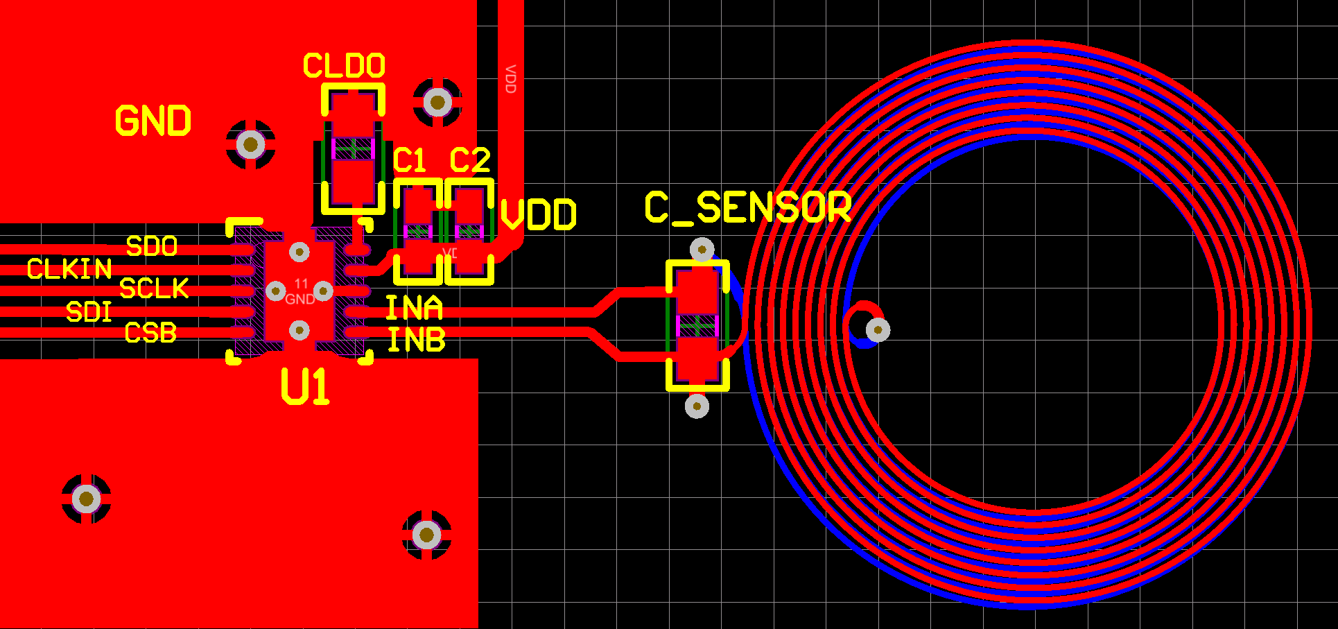
Ground and power planes are helpful for maintaining a clean supply to the LDC1101. In the layout shown in Figure 61, a top-layer ground fill is also used for improved grounding.
11.1.2 CLKIN Routing
The CLKIN pin routing must maintain consistent impedance; typically this is 50 Ω, but can be adjusted based on board geometries. If a parallel termination resistor is used, it must be placed as close to the CLKIN pin as possible. Minimize layer changes and routing through vias for the CLKIN signal. Maintain an uninterrupted ground plane under the trace.
11.1.3 Capacitor Placement
The capacitor CLDO must be placed as close to the CLDO pin as possible.
Place the bypass capacitors as close to the VDD pin as possible, with the smaller valued capacitor placed closer.
11.1.4 Sensor Connections
The sensor capacitor must be as close to the sensor inductor as possible. The INA and INB traces must be routed in parallel and as close to each other as possible to minimize coupling of noise. If cable is to be used, then INA and INB should be a twisted pair or in coaxial cable. The distance between the INA/INB pins and the sensor affects the maximum possible sensor frequency. For some applications, it may be helpful to place small-value capacitor (for example, 10 pF) from INA to ground and INB to ground; these capacitors should be located close to the INA and INB pins.
Refer to Application Note LDC Sensor Design (SNOA930) for additional information on sensor design.
11.2 Layout Example
 Figure 61. Layout Recommendations