SLOS012C March 1987 – March 2016 LF353
PRODUCTION DATA.
- 1 Features
- 2 Applications
- 3 Description
- 4 Revision History
- 5 Pin Configuration and Functions
- 6 Specifications
- 7 Parameter Measurement Information
- 8 Detailed Description
- 9 Application and Implementation
- 10Power Supply Recommendations
- 11Layout
- 12Device and Documentation Support
- 13Mechanical, Packaging, and Orderable Information
Package Options
Refer to the PDF data sheet for device specific package drawings
Mechanical Data (Package|Pins)
- D|8
- P|8
Thermal pad, mechanical data (Package|Pins)
Orderable Information
9 Application and Implementation
NOTE
Information in the following applications sections is not part of the TI component specification, and TI does not warrant its accuracy or completeness. TI’s customers are responsible for determining suitability of components for their purposes. Customers should validate and test their design implementation to confirm system functionality.
9.1 Application Information
The LF353 has two independent amplifiers that have very low input bias current which allow using higher resistance resistors in the feedback network. The upper input common mode range goes to the upper supply rail. The lower common mode range does not include the negative supply rail. Output resistance is 200 ohms to protect the device from accidental shorts.
9.2 Typical Application
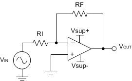
A typical application for an operational amplifier is an inverting amplifier. This amplifier takes a positive voltage on the input, and makes it a negative voltage. In the same manner, it also makes negative voltages positive.
 Figure 5. Inverting Amplifier
9.2.1 Design Requirements
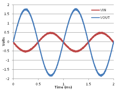
The supply voltage must be chosen such that it is larger than the input voltage range and output range. For instance, this application scales a signal of ±0.5 V to ±1.8 V. Setting the supply at ±12 V is sufficient to accommodate this application.
9.2.2 Detailed Design Procedure
Determine the gain required by the inverting amplifier using Equation 1 and Equation 2.


Once the desired gain is determined, choose a value for RI or RF. Choosing a value in the kΩ range is desirable because the amplifier circuit uses currents in the mA range. This ensures the part does draw too much current. For this example, choose 10 kΩ for RI and 36 kΩ for RF, as shown in Equation 3.

9.2.3 Application Curve
 Figure 6. Input and Output Voltages of the Inverting Amplifier