SNOSD56 June 2017 LF412-N-MIL
PRODUCTION DATA.
- 1 Features
- 2 Applications
- 3 Description
- 4 Revision History
- 5 Pin Configuration and Functions
- 6 Specifications
- 7 Detailed Description
- 8 Application and Implementation
- 9 Power Supply Recommendations
- 10Layout
- 11Device and Documentation Support
- 12Mechanical, Packaging, and Orderable Information
Package Options
Mechanical Data (Package|Pins)
- LMC|8
Thermal pad, mechanical data (Package|Pins)
Orderable Information
6 Specifications
6.1 Absolute Maximum Ratings
over operating free-air temperature range (unless otherwise noted)(1)| MIN | MAX | UNIT | ||
|---|---|---|---|---|
| Supply voltage | –18 | 18 | V | |
| Differential input voltage | –30 | 30 | V | |
| Input voltage range | ||||
| Output short circuit duration | Continuous | |||
| Power dissipation | 670 | mW | ||
| TJ maximum | 115 | °C | ||
| Operating temperature range | See Thermal Information | |||
| Storage temperature, Tstg | −65 | 150 | °C | |
(1) Stresses beyond those listed under Absolute Maximum Ratings may cause permanent damage to the device. These are stress ratings only, which do not imply functional operation of the device at these or any other conditions beyond those indicated under Recommended Operating Conditions. Exposure to absolute-maximum-rated conditions for extended periods may affect device reliability.
6.2 ESD Ratings
| VALUE | UNIT | |||
|---|---|---|---|---|
| V(ESD) | Electrostatic discharge | Human-body model (HBM), per ANSI/ESDA/JEDEC JS-001(1) | ±1700 | V |
| Charged-device model (CDM), per JEDEC specification JESD22-C101(2) | ±1700 | |||
(1) JEDEC document JEP155 states that 500-V HBM allows safe manufacturing with a standard ESD control process. Manufacturing with less than 500-V HBM is possible with the necessary precautions. Pins listed as ±1700 V may actually have higher performance.
(2) JEDEC document JEP157 states that 250-V CDM allows safe manufacturing with a standard ESD control process. Manufacturing with less than 250-V CDM is possible with the necessary precautions. Pins listed as ±1700 V may actually have higher performance.
6.3 Recommended Operating Conditions
over operating free-air temperature range (unless otherwise noted)| MIN | NOM | MAX | UNIT | ||
|---|---|---|---|---|---|
| Supply voltage | ±15 | V | |||
6.4 Thermal Information
| THERMAL METRIC(1) | LF412-N-MIL | UNIT | ||
|---|---|---|---|---|
| LMC (TO) | P (PDIP) | |||
| 8 PINS | 8 PINS | |||
| RθJA | Junction-to-ambient thermal resistance (typical) | 152 | 115 | °C/W |
(1) For more information about traditional and new thermal metrics, see the Semiconductor and IC Package Thermal Metrics application report.
6.5 DC Electrical Characteristics
over operating free-air temperature range (unless otherwise noted)| PARAMETER | TEST CONDITIONS | LF412-N-MIL(1) | UNIT | ||||
|---|---|---|---|---|---|---|---|
| MIN | TYP | MAX | |||||
| VOS | Input offset voltage | RS =10 kΩ, TA = 25°C | 1 | 3 | mV | ||
| ΔVOS/ΔT | Average TC of input offset voltage | RS = 10 kΩ | 7 | μV/°C | |||
| IOS | Input offset current | VS = ±15 V(2) | TJ = 25°C | 25 | 100 | pA | |
| TJ = 70°C | 2 | nA | |||||
| TJ = 125°C | 25 | nA | |||||
| IB | Input bias current | VS=±15V(2)(2) | TJ = 25°C | 50 | 200 | pA | |
| TJ = 70°C | 4 | nA | |||||
| TJ = 125°C | 50 | nA | |||||
| RIN | Input resistance | TJ = 25°C | 1012 | Ω | |||
| AVOL | Large signal voltage gain |
RL = 2 k, TA = 25°C, VS = ±15 V, VO = ±10 V | 25 | 200 | V/mV | ||
| Over temperature | 15 | 200 | |||||
| VO | Output voltage swing | VS = ±15 V, RL = 10 k | ±12 | ±13.5 | V | ||
| VCM | Input common-mode voltage range | ±11 | 14.5 | V | |||
| −11.5 | V | ||||||
| CMRR | Common-mode rejection ratio |
RS ≤ 10 k | 70 | 100 | dB | ||
| PSRR | Supply voltage rejection ratio |
(3) | 70 | 100 | dB | ||
| IS | Supply current | VO = 0 V, RL = ∞ | 3.6 | 6.5 | mA | ||
(1) Unless otherwise specified, the specifications apply over the full temperature range and for VS = ±15 V for the LF412-N-MIL. VOS, IB, and IOS are measured at VCM = 0.
(2) The input bias currents are junction leakage currents which approximately double for every 10°C increase in the junction temperature, TJ. Due to limited production test time, the input bias currents measured are correlated to junction temperature. In normal operation the junction temperature rises above the ambient temperature as a result of internal power dissipation, PD. TJ = TA + θJA PD where θJA is the thermal resistance from junction to ambient. Use of a heat sink is recommended if input bias current is to be kept to a minimum.
(3) Supply voltage rejection ratio is measured for both supply magnitudes increasing or decreasing simultaneously in accordance with common practice. VS = ±6 V to ±15 V.
6.6 AC Electrical Characteristics
over operating free-air temperature range (unless otherwise noted)| PARAMETER | TEST CONDITIONS | LF412-N-MIL(1) | UNIT | |||
|---|---|---|---|---|---|---|
| MIN | TYP | MAX | ||||
| Amplifier to amplifier coupling |
TA = 25°C f = 1 Hz – 20 kHz (Input referred) |
−120 | dB | |||
| SR | Slew rate | VS = ±15 V TA = 25°C |
8 | 15 | V/μs | |
| GBW | Gain-bandwidth product | VS = ±15 V TA = 25°C |
2.7 | 4 | MHz | |
| THD | Total harmonic dist | AV = 10 RL = 10 k VO = 20 Vp-p BW = 20 Hz – 20 kHz |
≤0.02% | |||
| en | Equivalent input noise voltage |
TA = 25°C RS = 100 Ω f = 1 kHz |
25 | nV / √Hz | ||
| in | Equivalent input noise current |
TA = 25°C, f = 1 kHz | 0.01 | pA / √Hz | ||
(1) Unless otherwise specified, the specifications apply over the full temperature range and for VS = ±15 V for the LF412-N-MIL. VOS, IB, and IOS are measured at VCM = 0.
6.7 Typical Characteristics
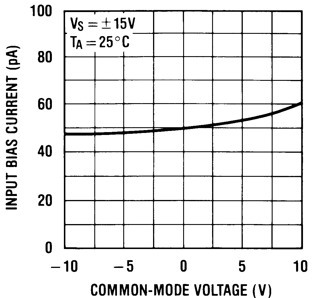
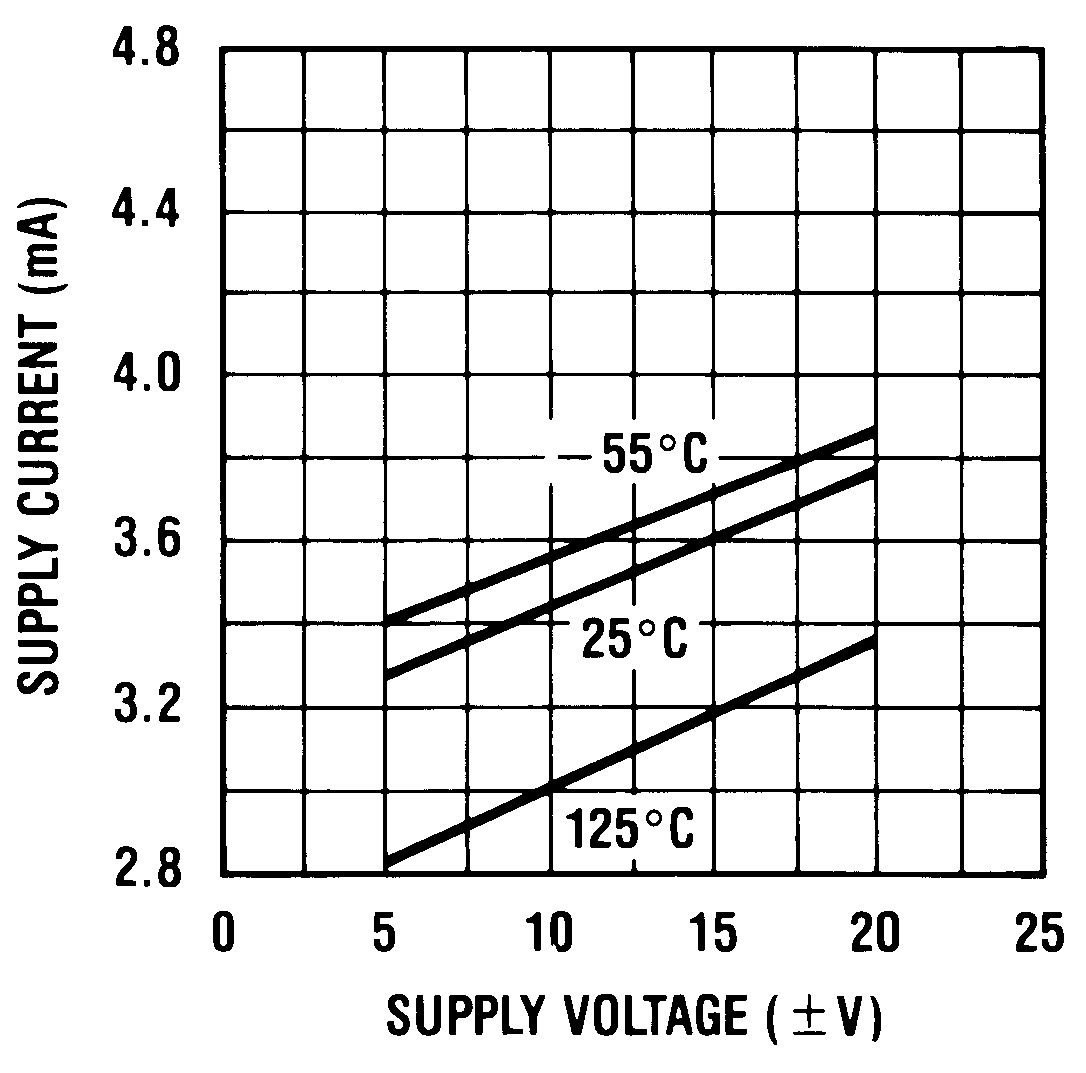
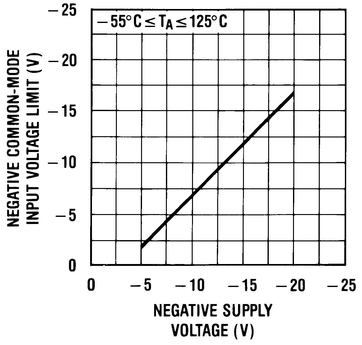
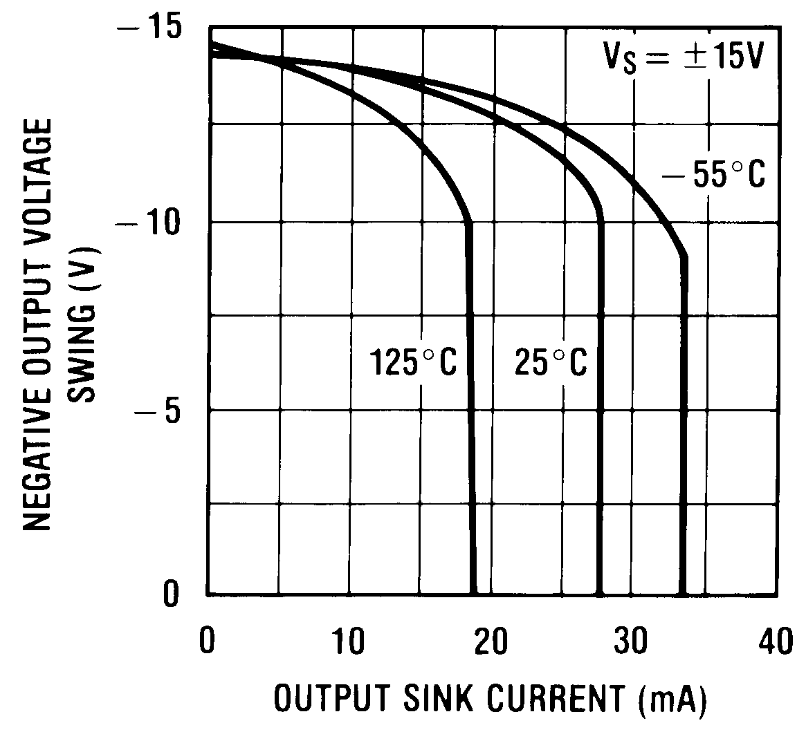
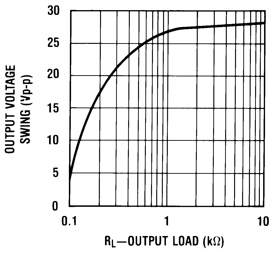
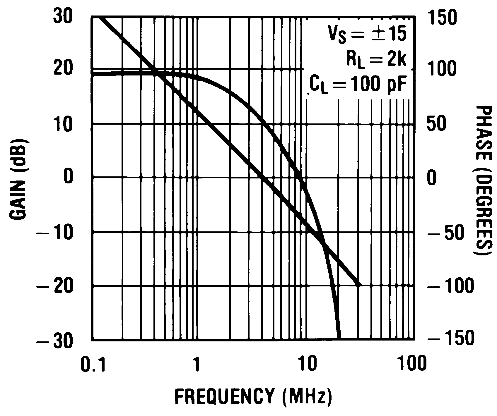
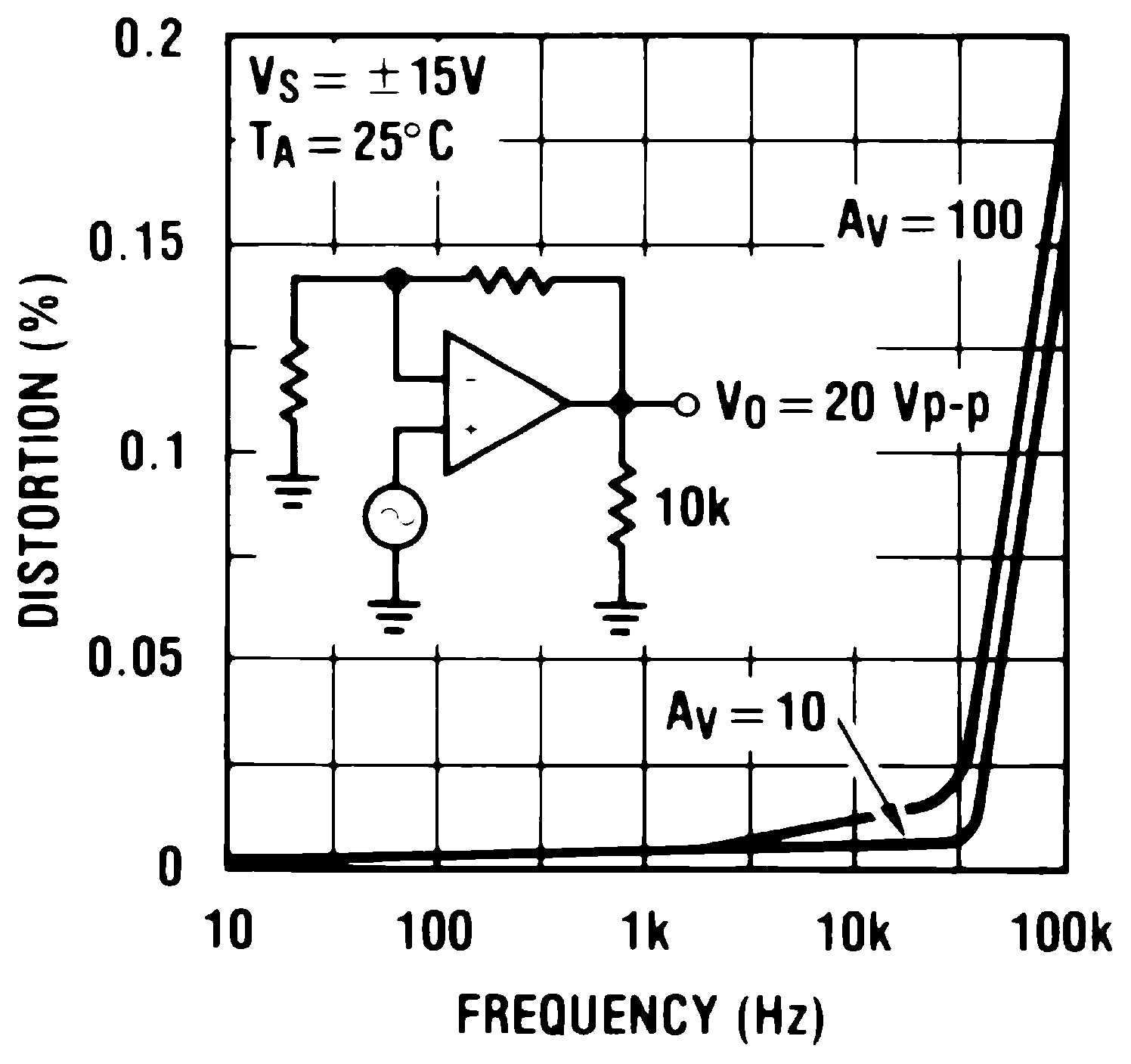
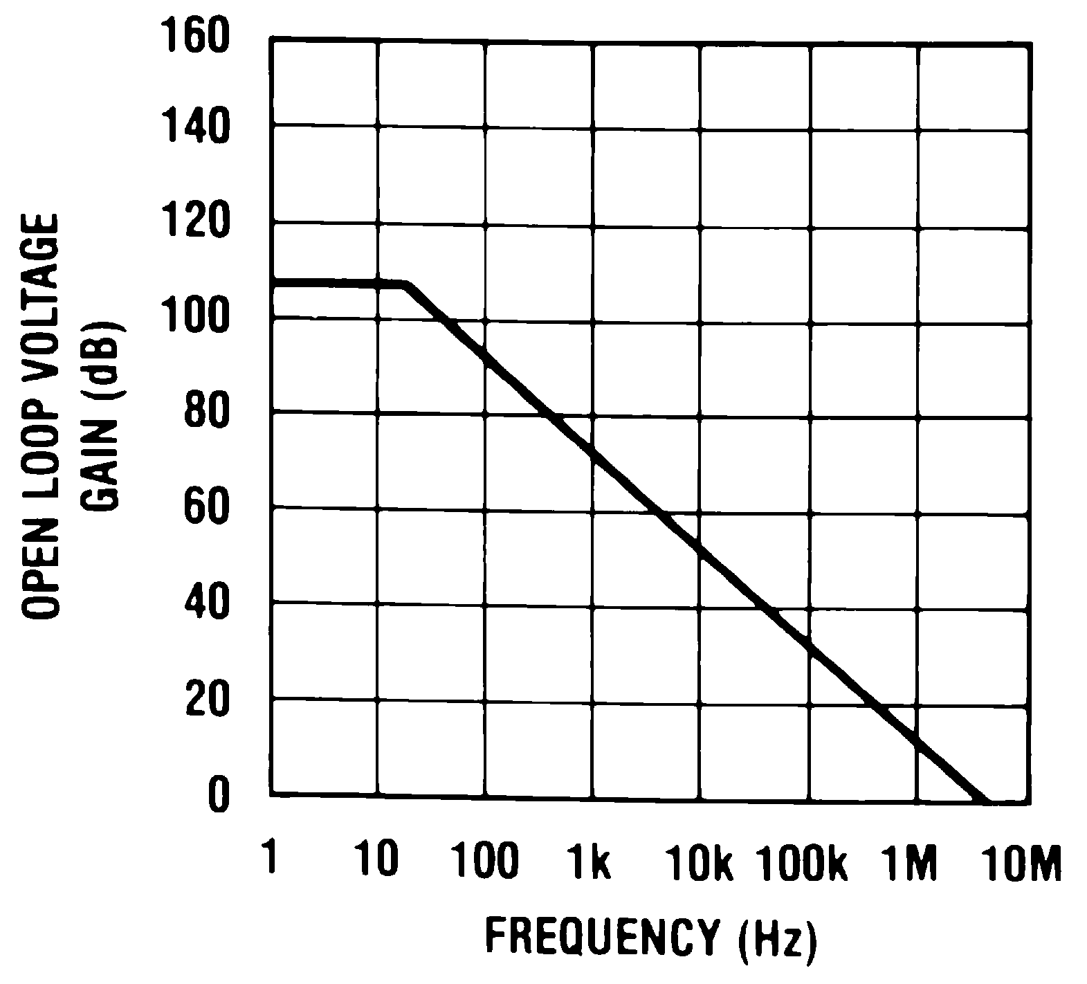
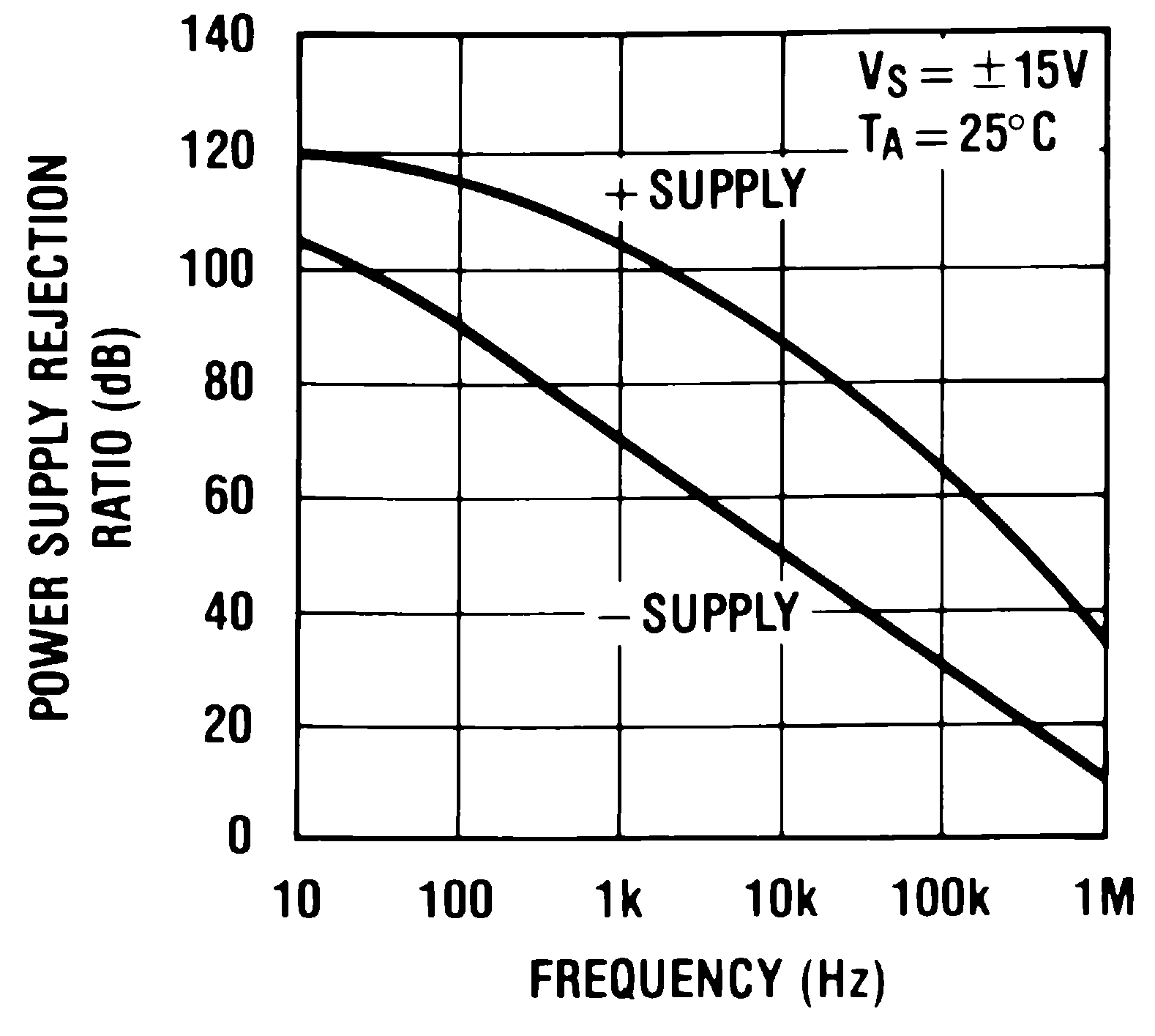
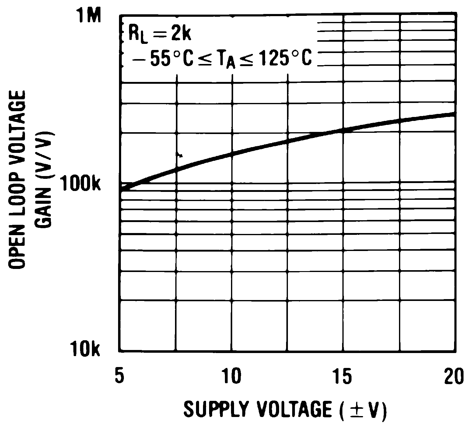
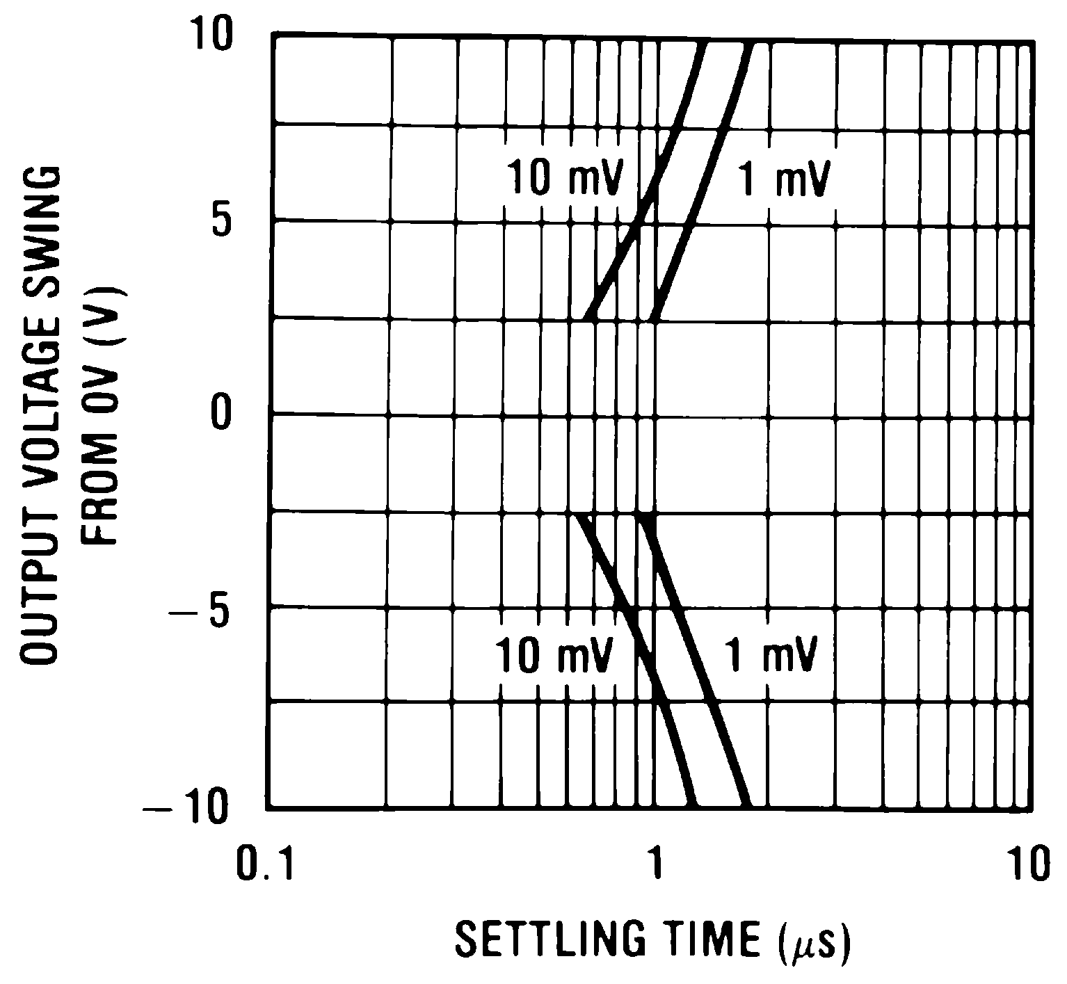
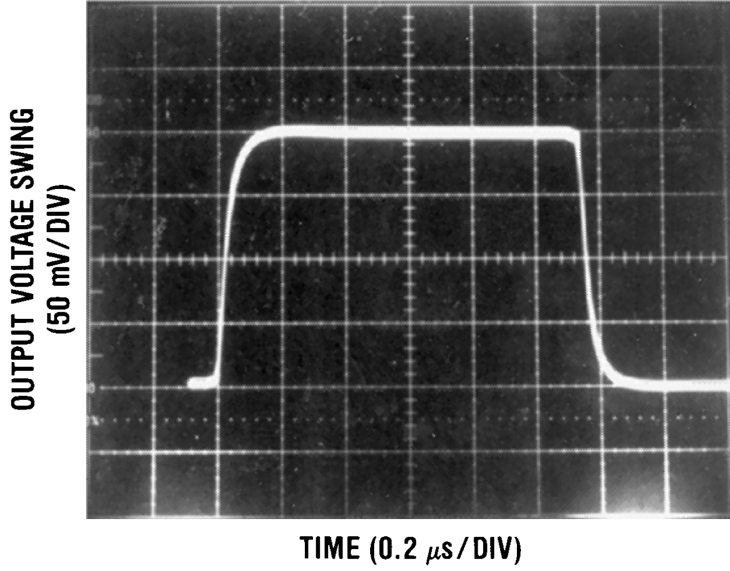
| RL = 2 kΩ | CL = 10 pF |
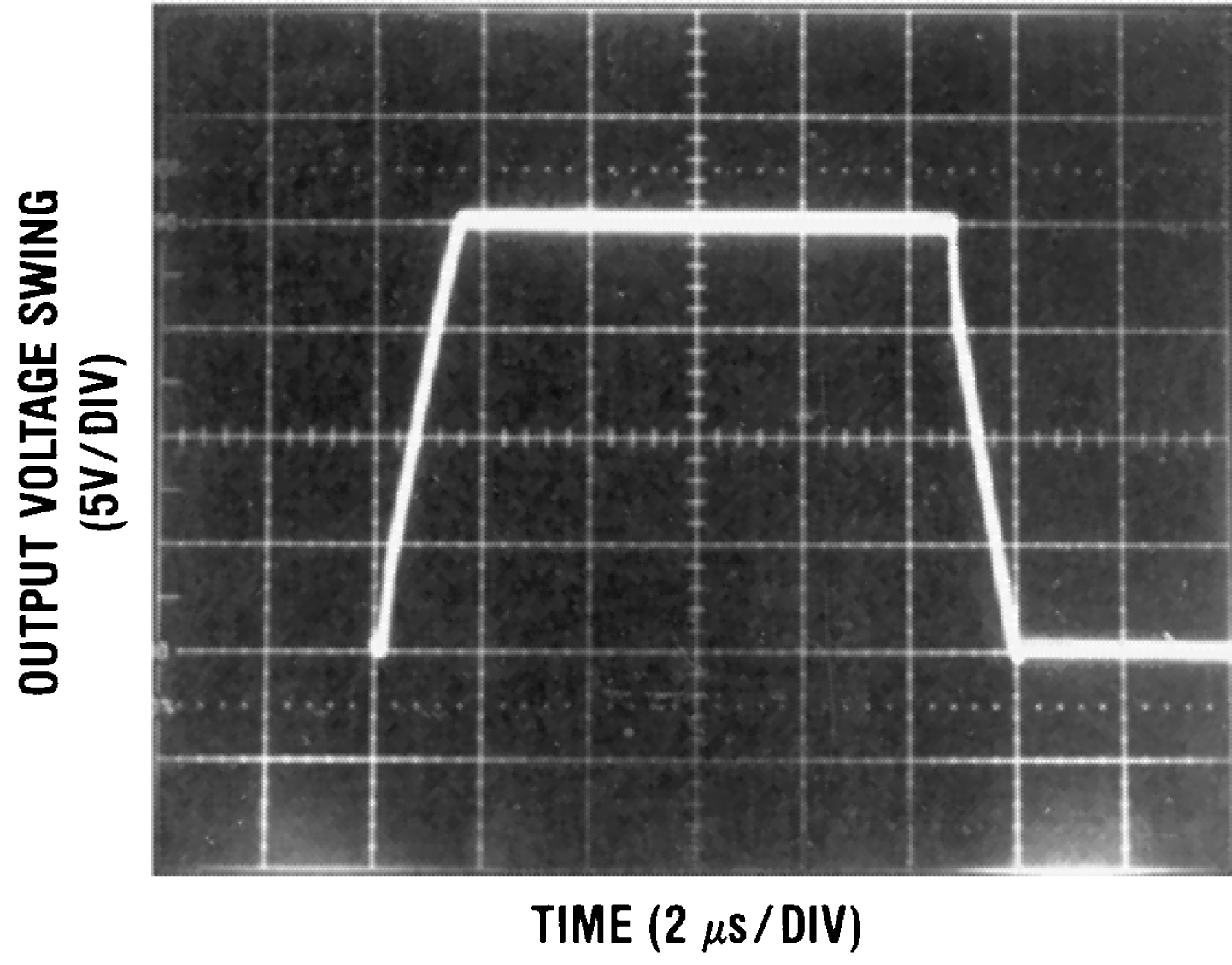
| RL = 2 kΩ | CL = 10 pF |
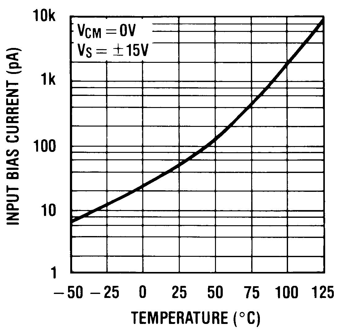
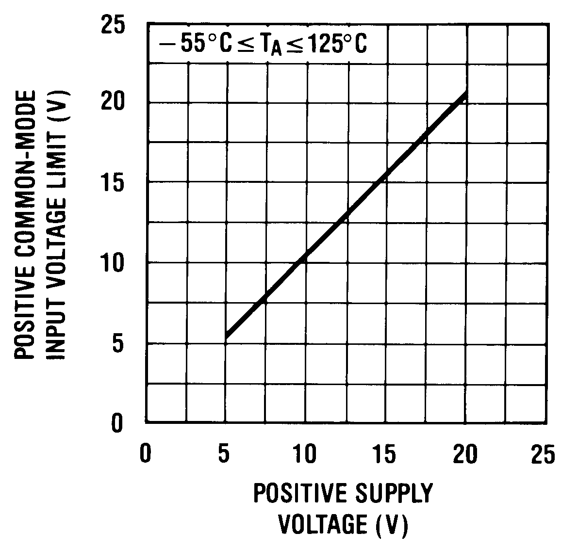
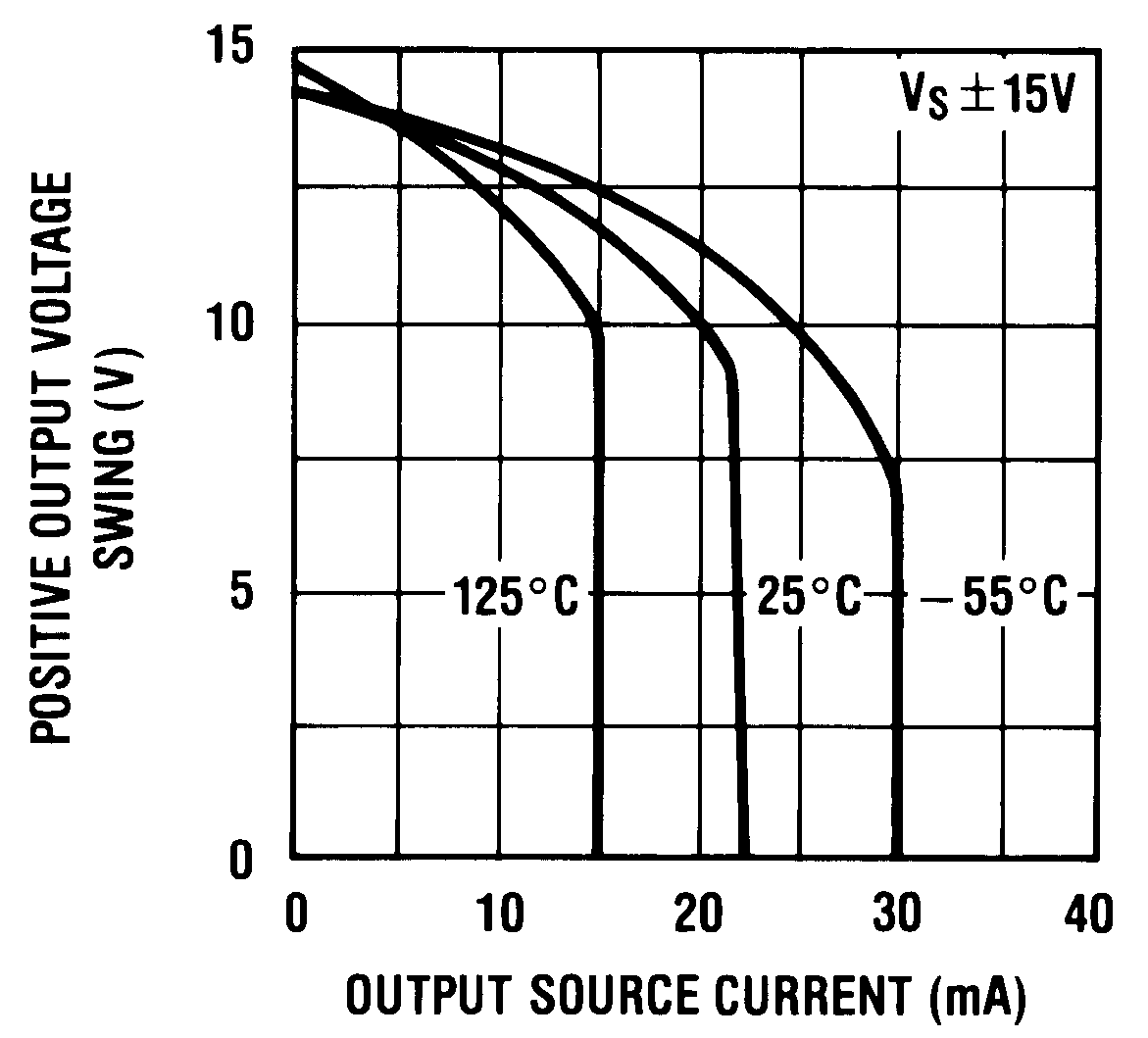
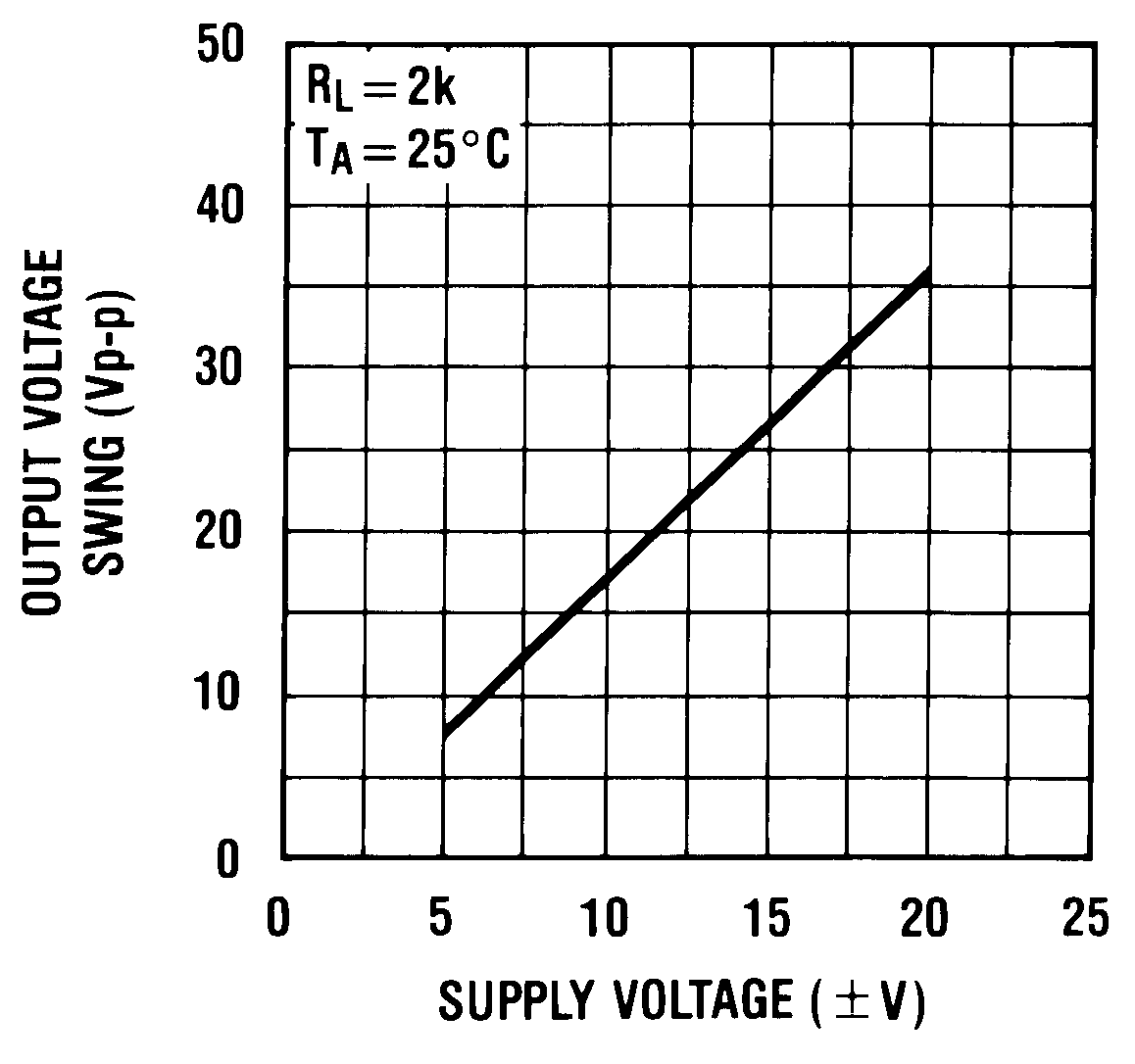
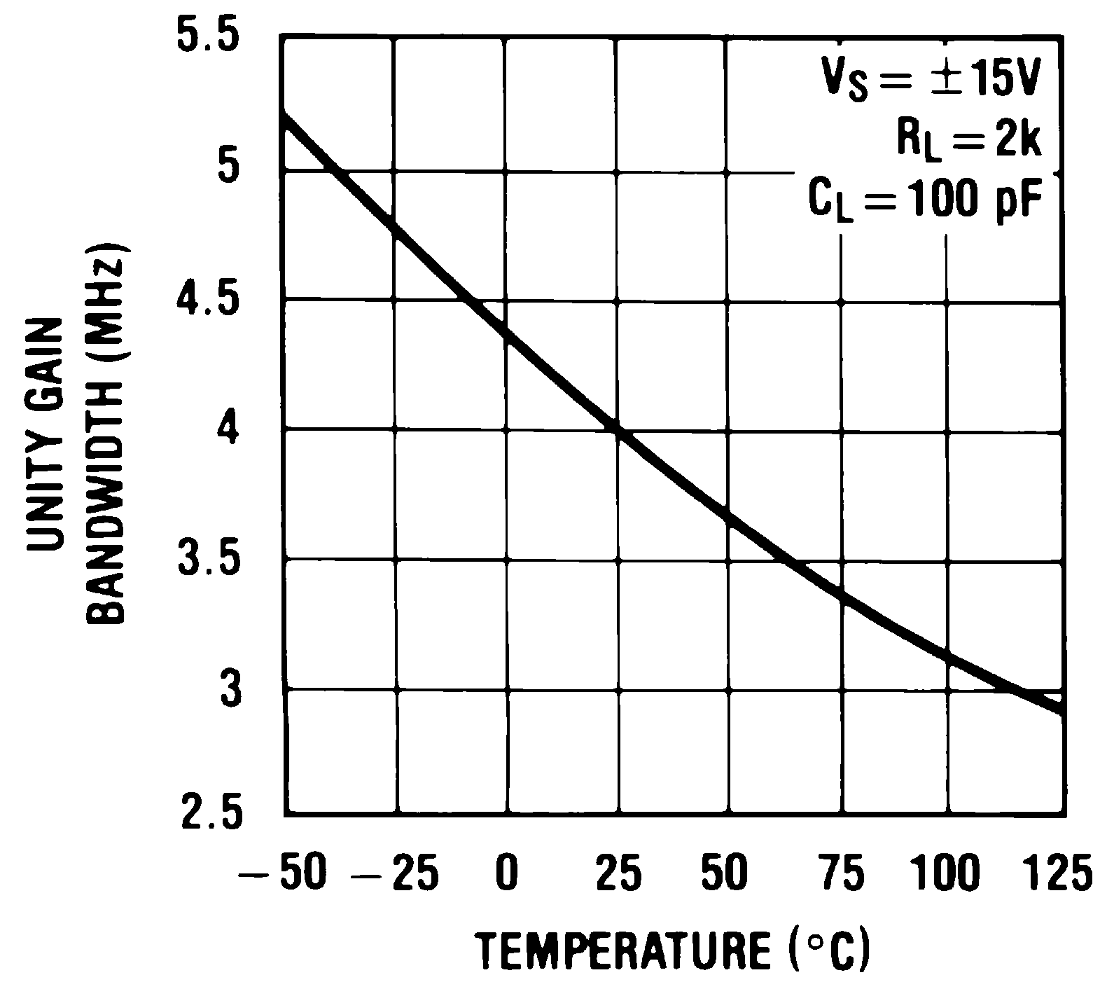
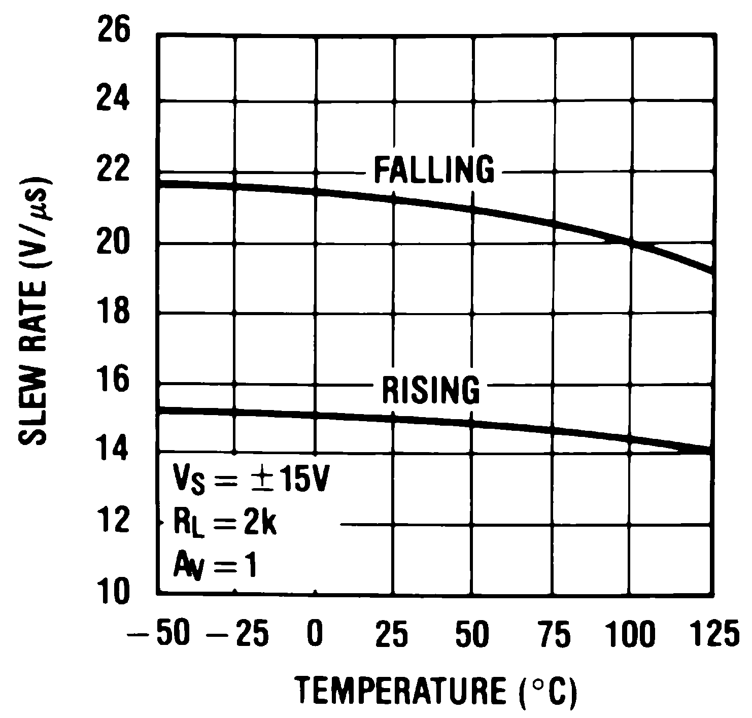
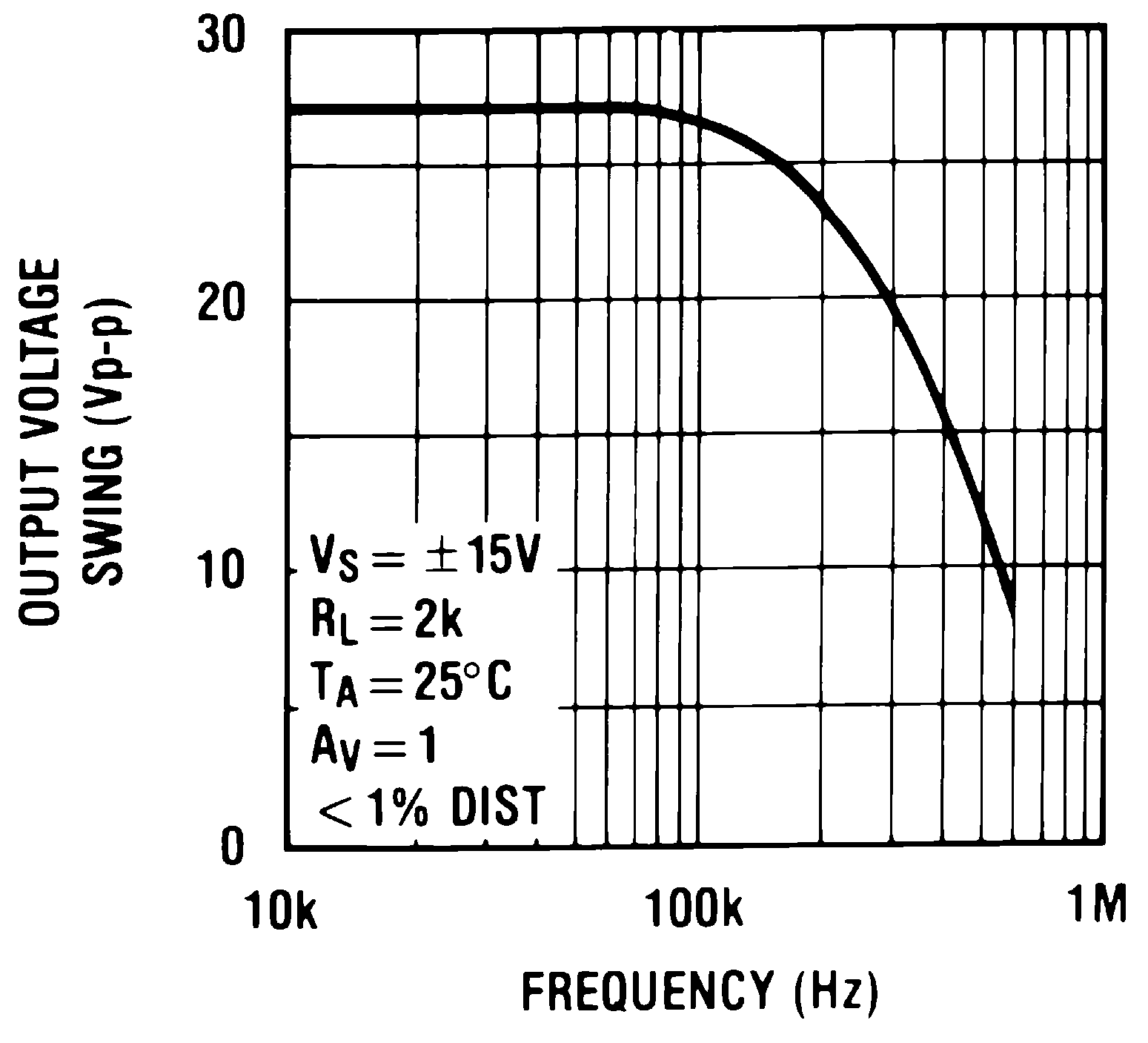
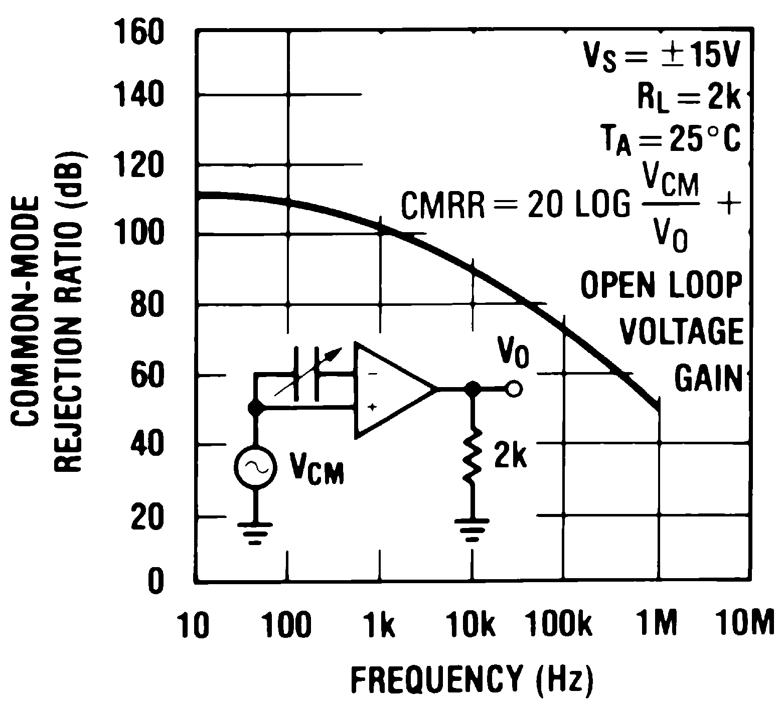
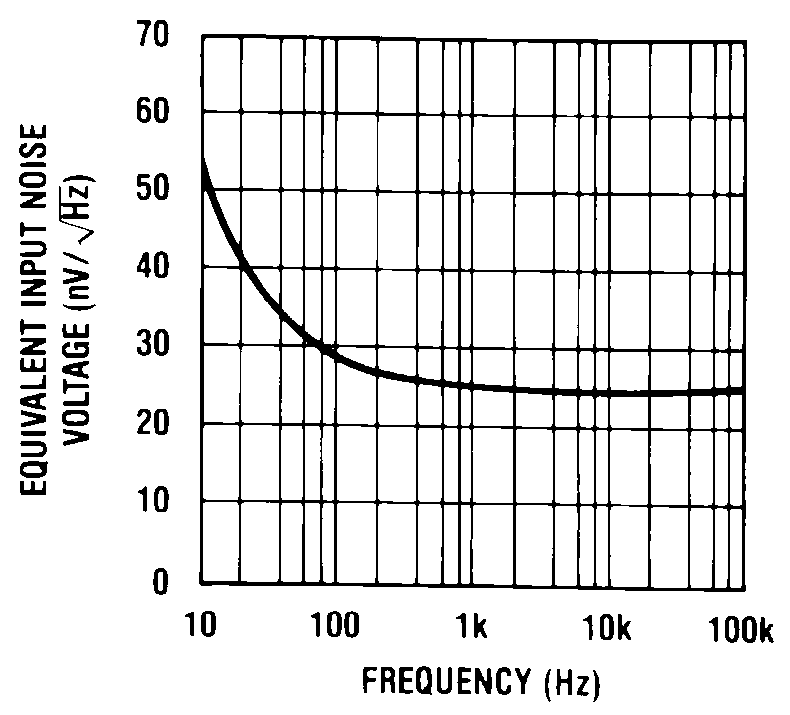
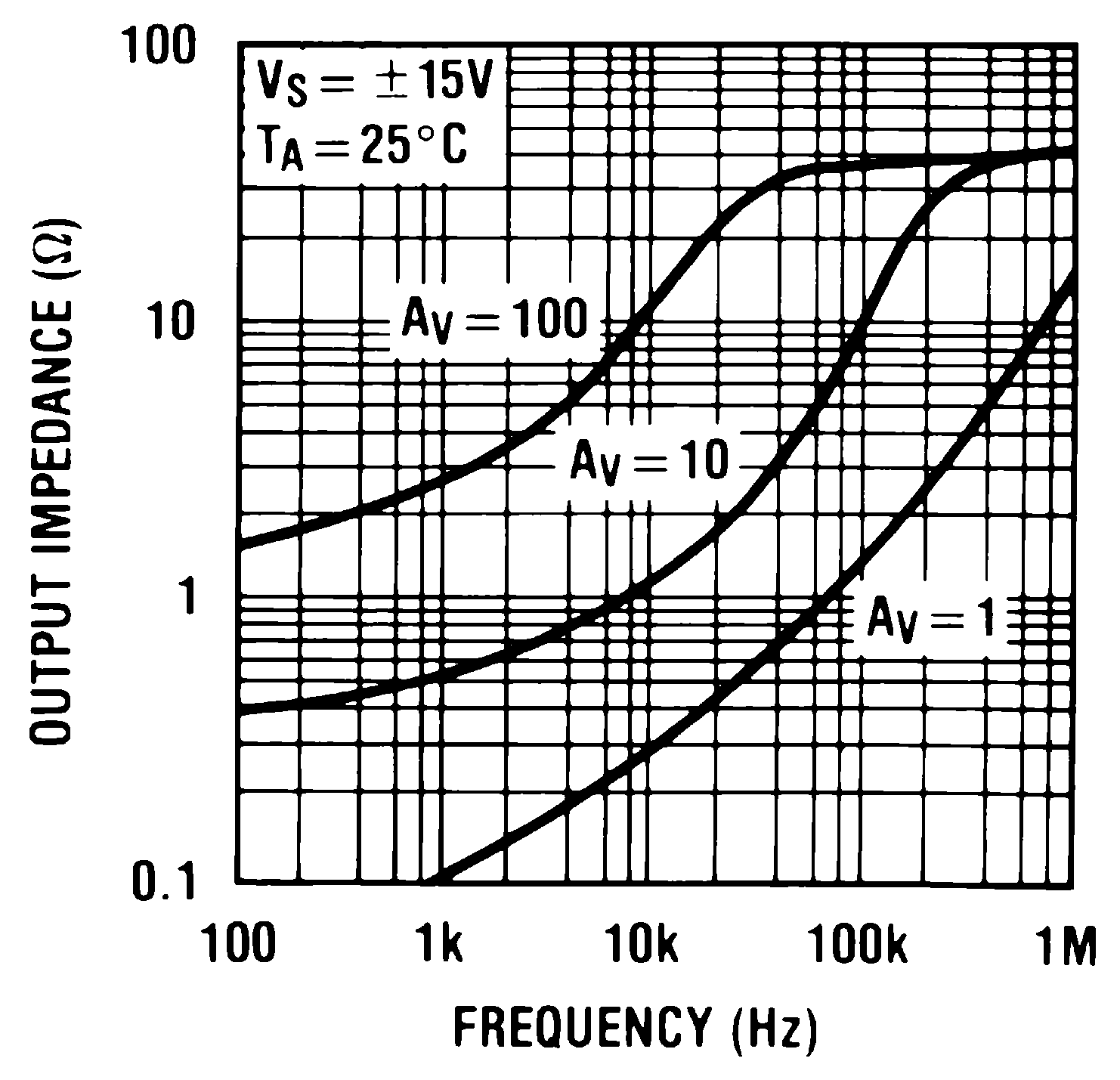
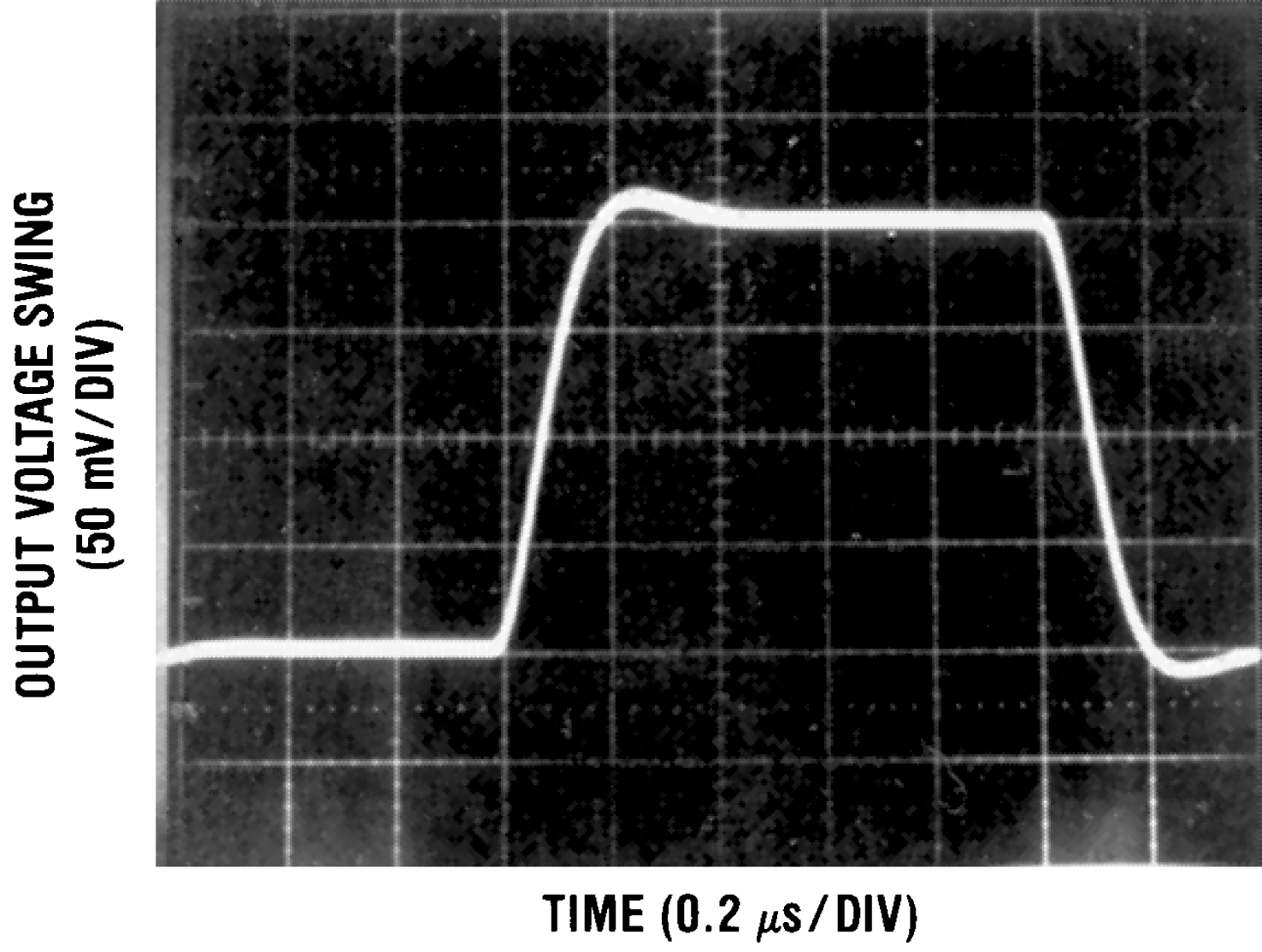
| RL = 2 kΩ | CL = 10 pF | |
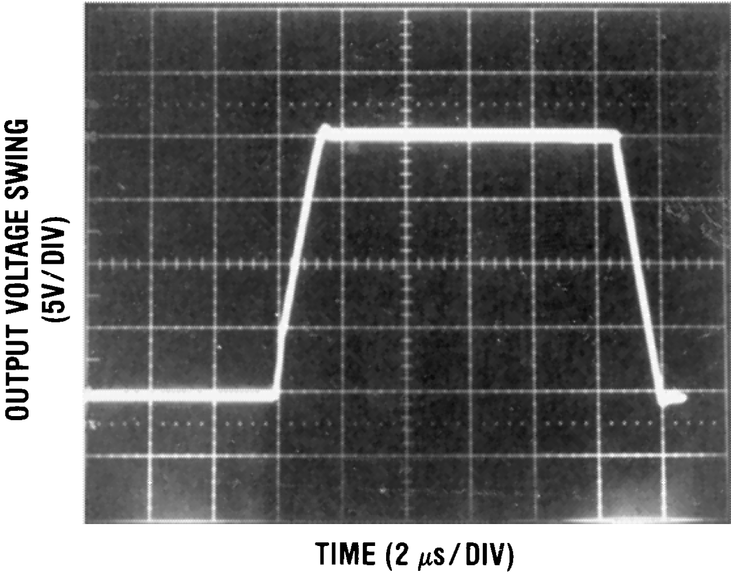
| RL = 2 kΩ | CL = 10 pF |
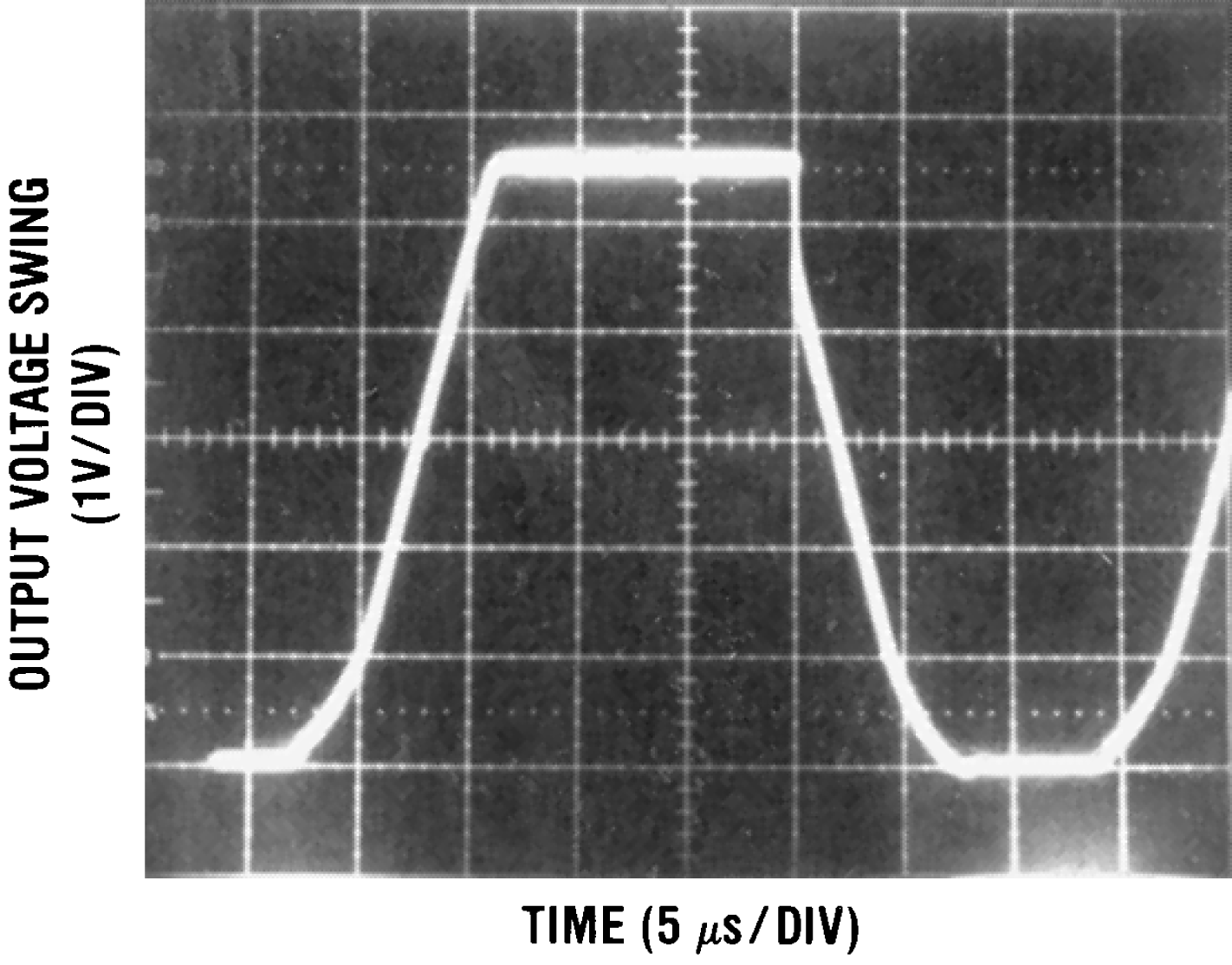
| RL = 100 Ω | CL = 10 pF |